- 您现在的位置:买卖IC网 > PDF目录383294 > M366S3354BTS-C7A (SAMSUNG SEMICONDUCTOR CO. LTD.) SDRAM Unbuffered Module 168pin Unbuffered Module based on 512Mb B-die 62/72-bit Non ECC/ECC PDF资料下载
参数资料
| 型号: | M366S3354BTS-C7A |
| 厂商: | SAMSUNG SEMICONDUCTOR CO. LTD. |
| 英文描述: | SDRAM Unbuffered Module 168pin Unbuffered Module based on 512Mb B-die 62/72-bit Non ECC/ECC |
| 中文描述: | 内存缓冲模块168线缓冲模块基于512Mb乙芯片62/72-bit非ECC / ECC的 |
| 文件页数: | 5/22页 |
| 文件大小: | 379K |
| 代理商: | M366S3354BTS-C7A |
256MB, 512MB, 1GB Unbuffered DIMM
Rev. 1.1 February 2004
SDRAM
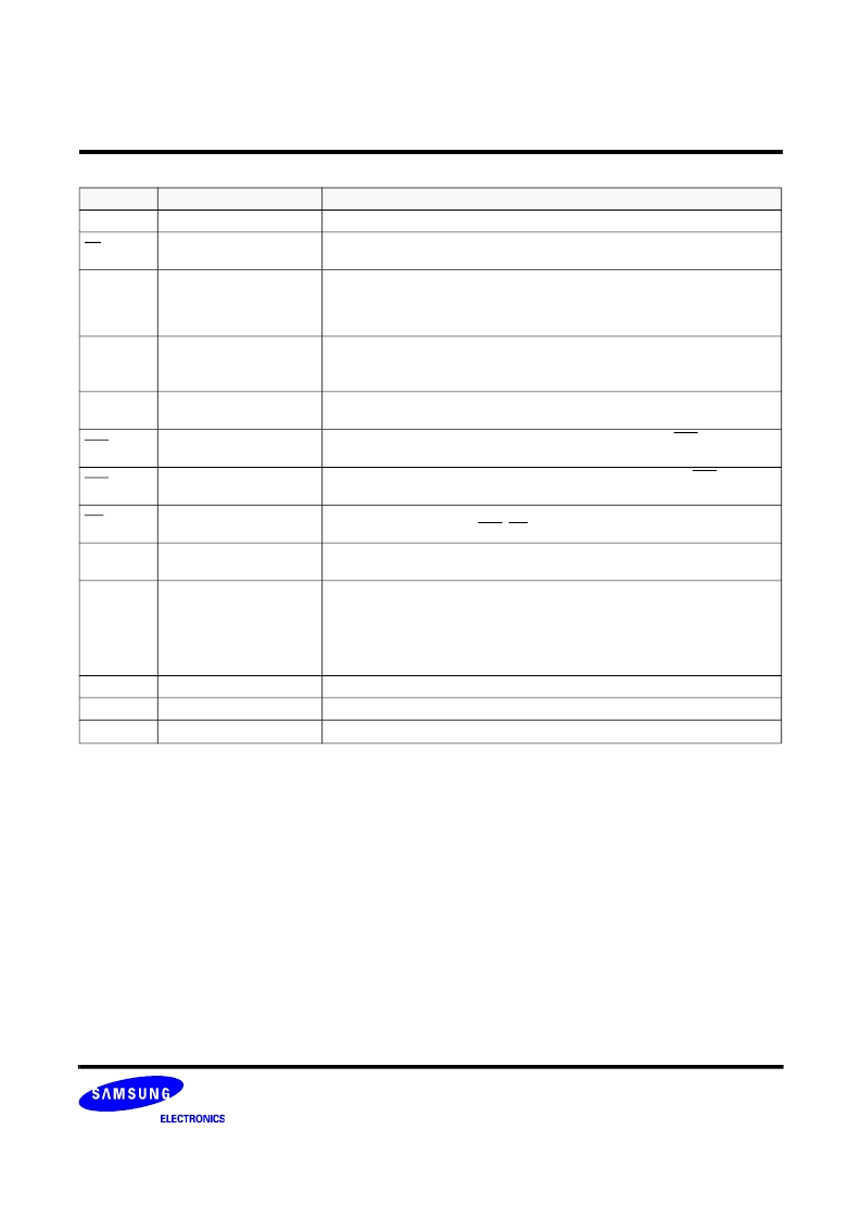
PIN CONFIGURATION DESCRIPTION
Pin
Name
Input Function
CLK
System clock
Active on the positive going edge to sample all inputs.
CS
Chip select
Disables or enables device operation by masking or enabling all inputs except
CLK, CKE and DQM
CKE
Clock enable
Masks system clock to freeze operation from the next clock cycle.
CKE should be enabled at least one cycle prior to new command.
Disable input buffers for power down in standby.
CKE should be enabled 1CLK+tss prior to valid command.
A0 ~ A12
Address
Row/column addresses are multiplexed on the same pins.
Row address : RA0 ~ RA12
Column address x8 CA0 ~ CA9, CA11), x16 CA0 ~ CA9)
BA0 ~ BA1
Bank select address
Selects bank to be activated during row address latch time.
Selects bank for read/write during column address latch time.
RAS
Row address strobe
Latches row addresses on the positive going edge of the CLK with RAS low.
Enables row access & precharge.
CAS
Column address strobe
Latches column addresses on the positive going edge of the CLK with CAS low.
Enables column access.
WE
Write enable
Enables write operation and row precharge.
Latches data in starting from CAS, WE active.
DQM0 ~ 7
Data input/output mask
Makes data output Hi-Z, t
SHZ
after the clock and masks the output.
Blocks data input when DQM active. (Byte masking)
REGE
Register enable
The device operates in the transparent mode when REGE is low. When REGE is high,
the device operates in the registered mode. In registered mode, the Address and con-
trol inputs are latched if CLK is held at a high or low logic level. the inputs are stored in
the latch/flip-flop on the rising edge of CLK. REGE is tied to V
DD
through 10K ohm
Resistor on PCB. So if REGE of module is floating, this module will be operated as reg-
istered mode.
DQ0 ~ 63
Data input/output
Data inputs/outputs are multiplexed on the same pins.
CB0 ~ 7
Check bit
Check bits for ECC.
V
DD
/V
SS
Power supply/ground
Power and ground for the input buffers and the core logic.
相关PDF资料 |
PDF描述 |
|---|---|
| M366S6553BTS-C7A | SDRAM Unbuffered Module 168pin Unbuffered Module based on 512Mb B-die 62/72-bit Non ECC/ECC |
| M374S2953BTS-C7A | SDRAM Unbuffered Module 168pin Unbuffered Module based on 512Mb B-die 62/72-bit Non ECC/ECC |
| M366S3253BTS | 32Mx64 SDRAM DIMM based on 32Mx8, 4Banks, 8K Refresh, 3.3V Synchronous DRAMs with SPD |
| M366S3253BTS-C75 | 32Mx64 SDRAM DIMM based on 32Mx8, 4Banks, 8K Refresh, 3.3V Synchronous DRAMs with SPD |
| M366S3323DTS | 32Mx64 SDRAM DIMM based on 16Mx8, 4Banks, 4K Refresh, 3.3V Synchronous DRAMs with SPD |
相关代理商/技术参数 |
参数描述 |
|---|---|
| M366S3953MTS-C1H | 制造商:SAMSUNG 制造商全称:Samsung semiconductor 功能描述:PC133/PC100 Unbuffered DIMM |
| M366S6453AT0-C1H00 | 制造商:Samsung SDI 功能描述:64M X 64 SDRAM DIMM based on 32M X 8, 4banks, 8K refresh, 3.3V synchronous drams with spd |
| M366S6453CTS | 制造商:SAMSUNG 制造商全称:Samsung semiconductor 功能描述:PC133/PC100 Unbuffered DIMM |
| M366S6453CTS-L1H/C1H | 制造商:SAMSUNG 制造商全称:Samsung semiconductor 功能描述:PC133/PC100 Unbuffered DIMM |
| M366S6453CTS-L1L/C1L | 制造商:SAMSUNG 制造商全称:Samsung semiconductor 功能描述:PC133/PC100 Unbuffered DIMM |
发布紧急采购,3分钟左右您将得到回复。