- 您现在的位置:买卖IC网 > PDF目录67762 > M37161EFSP 8-BIT, OTPROM, 8 MHz, MICROCONTROLLER, PDIP42 PDF资料下载
参数资料
| 型号: | M37161EFSP |
| 元件分类: | 微控制器/微处理器 |
| 英文描述: | 8-BIT, OTPROM, 8 MHz, MICROCONTROLLER, PDIP42 |
| 封装: | 0.600 INCH, 1.78 MM PITCH, PLASTIC, SDIP-42 |
| 文件页数: | 16/16页 |
| 文件大小: | 1024K |
| 代理商: | M37161EFSP |
Rev.1.00
2003.11.25
page 7 of 128
M37161M8/MA/MF-XXXSP/FP,M37161EFSP/FP
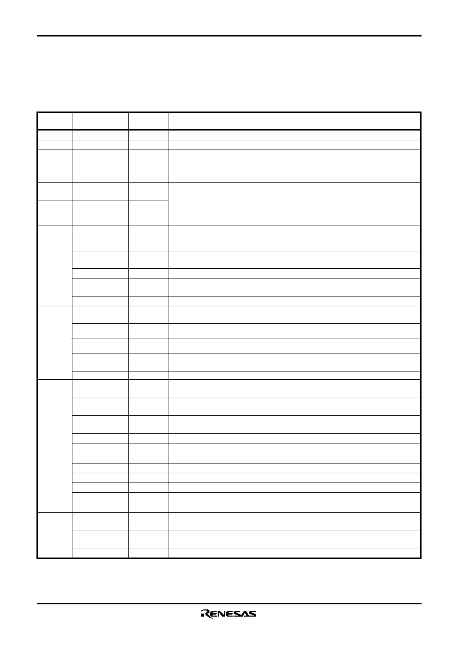
Pin
Name
Input/
Functions
Output
VCC, VSS
Power source
Apply voltage of 5 V ± 10 % to (typical) VCC, and 0 V to VSS.
CNVSS
This is connected to VSS.
______
RESET
Reset input
Input
To enter the reset state, the reset input pin must be kept at a LOW for 2 ms or more (under
normal VCC conditions).
If more time is needed for the quartz-crystal oscillator to stabilize, this LOW condition should
be maintained for the required time.
XIN
Clock input
Input
This is the input pin for the main clock generating circuit. Built-in clock clock generation
circuit, when set
XOUT
Clock output
Output
to oscillation frequency, connect ceramic resonator or crystal frequency between XIN and
XOUT. When use external clock input, connect clock oscillation source to XIN pin, and open
XOUT pin.
P00/PWM0/DA I/O port P0
I/O
Port P0 is a 8-bit I/O port with a direction register allowing each I/O bit to be individually
P01/PWM1,
programmed as input or output. At reset, this port is set to input mode. The output structure
P02/PWM2,
is N-channel open-drain output. (See note)
P03/PWM3/AD1,
8-bit
Output
Ouput Pins P00 to P04 are also used as 8-bit PWM output pins PWM0 to PWM4, respectively. The
P04/PWM4/AD2,
PWM output
output structure is N-channel open-drain output.
P05/AD3,
DA output
Output
P00 pin is also used as 14-bit PWM output pin DA. The output structure is CMOS.
P06/INT2/AD4,
External interrupt
Input
Pins P06 and P07 are also used as INT external interrupt input pins INT2 and INT1 respectively.
P07/INT1
input
Analog input
Input
Pins P03, P04, P05 and P06 are also used as analog input pins AD1, AD2, AD3 and AD4, respectively.
P10/CLK CONT, I/O port P1
I/O
Port P1 is a 7-bit I/O port and has basically the same functions as port P0. The output
P11/SCL1,
structure is CMOS output. (See note)
P12/SCL2,
Multi-master
I/O
Pins P11–P14 are used as SCL1, SCL2, SDA1 and SDA2 respectively, when multi-master
P13/SDA1,
I2C-BUS interface
I2C-BUS interface is used. The output structure is N-channel open-drain output.
P14/SDA2,
Clock control
Output
P10 pin is also used as Clock control output CLK CONT. The output structure is CMOS
P15,
output.
P16/AD8/TIM2
External clock
Input
P16 pin is also used as timer external clock input pin TIM2.
input for timer
Analog input
Input
P16 pin is also used as analog input pin AD8.
P20/SCLK/AD5,
I/O port P2
I/O
Port P2 is a 8-bit I/O port and has basically the same functions as port P0. The output
P21/SOUT/AD6,
structure is CMOS output. (See note)
P22/SIN/AD7,
Serial I/O synchronous
I/O
P20 pin is also used as serial I/O synchronous clock input/output pin SCLK. The output
P23/TIM3,
clock input/output port
structure is N-channel open-drain output.
P24/TIM2,
Serial I/O data
Output
P21 pin is also used as serial I/O data output pin SOUT. The output structure is open-drain
P25/INT3,
output
output.
P26/XCIN,
Serial I/O data input
Input
P22 pin is also used as serial I/O data input pin SIN.
P27/XCOUT
External clock
Input
Pins P23 and P24 are also used as timer external clock input pins TIM3 and TIM2
input for timer
respectively.
Analog input
Input
Pins P20–P22 are also used as analog input pins AD5, AD6 and AD7 respectively.
Sub-clock input
Input
P26 pin is also used as sub-clock input pin XCIN.
Sub-clock output
Output
P27 pin is also used as sub-clock output pin XCOUT. The output structure is CMOS output.
External interrupt
Input
P25 pin is also used as INT external interrupt input pin INT3.
input
P30/SDA3
I/O port P30, P31
I/O
Pins P30 and P31 are 2-bit I/O port and has basically the same functions as port P0.
P31/SCL3
The output structure is CMOS output. (See note)
P35-P37
Multi-master
I/O
Pins P30 and P31 are used as SDA3,SCL3 respectively, when multi-master I2C-BUS
I2C-BUS Interface
interface is used. The output structure is N-channel open-drain output.
Input P35-P37
Input
Pins P35–P37 are 3-bit input port.
7. PIN DESCRIPTION
Table 7.1 PIN DESCRIPTION
相关PDF资料 |
PDF描述 |
|---|---|
| M37161MF-XXXFP | 8-BIT, MROM, 8 MHz, MICROCONTROLLER, PDSO42 |
| M37161M8-XXXSP | 8-BIT, MROM, 8 MHz, MICROCONTROLLER, PDIP42 |
| M37212EFFP | 8-BIT, OTPROM, 8.1 MHz, MICROCONTROLLER, PQFP80 |
| M37212M8-XXXSP | 8-BIT, MROM, 8.1 MHz, MICROCONTROLLER, PDIP52 |
| M37212EFSP | 8-BIT, OTPROM, 8.1 MHz, MICROCONTROLLER, PDIP52 |
相关代理商/技术参数 |
参数描述 |
|---|---|
| M37161M8 | 制造商:RENESAS 制造商全称:Renesas Technology Corp 功能描述:SINGLE-CHIP 8-BIT CMOS MICROCOMPUTER |
| M37161M8-XXXFP | 制造商:RENESAS 制造商全称:Renesas Technology Corp 功能描述:SINGLE-CHIP 8-BIT CMOS MICROCOMPUTER |
| M37161M8-XXXSP | 制造商:RENESAS 制造商全称:Renesas Technology Corp 功能描述:SINGLE-CHIP 8-BIT CMOS MICROCOMPUTER |
| M37161MA-XXXFP | 制造商:RENESAS 制造商全称:Renesas Technology Corp 功能描述:SINGLE-CHIP 8-BIT CMOS MICROCOMPUTER |
| M37161MA-XXXSP | 制造商:RENESAS 制造商全称:Renesas Technology Corp 功能描述:SINGLE-CHIP 8-BIT CMOS MICROCOMPUTER |
发布紧急采购,3分钟左右您将得到回复。