- 您现在的位置:买卖IC网 > PDF目录80530 > M37510E6FS 8-BIT, UVPROM, 4 MHz, MICROCONTROLLER, CQCC160 PDF资料下载
参数资料
| 型号: | M37510E6FS |
| 元件分类: | 微控制器/微处理器 |
| 英文描述: | 8-BIT, UVPROM, 4 MHz, MICROCONTROLLER, CQCC160 |
| 文件页数: | 32/44页 |
| 文件大小: | 469K |
| 代理商: | M37510E6FS |
第1页第2页第3页第4页第5页第6页第7页第8页第9页第10页第11页第12页第13页第14页第15页第16页第17页第18页第19页第20页第21页第22页第23页第24页第25页第26页第27页第28页第29页第30页第31页当前第32页第33页第34页第35页第36页第37页第38页第39页第40页第41页第42页第43页第44页
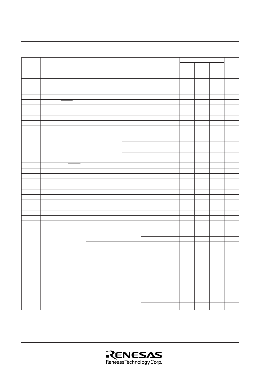
37
7510 Group
SINGLE-CHIP 8-BIT CMOS MICROCOMPUTER
MITSUBISHI MICROCOMPUTERS
Parameter
“H” output voltage P00–P07, P10–P17, P20–P27,
P30–P37, P41–P47, P50, P51
“L” output voltage P00–P07, P10–P17, P20–P27,
P30–P37, P41–P47, P50, P51
Hysteresis INT0, INT1, CNTR0, CNTR1
Hysteresis SCLK1, SCLK2, RXD1, RXD2
Hysteresis RESET
“H” input current P00–P07, P10–P17, P20–P27,
P30–P37, P41–P47, P50, P51
“H” input current RESET, P40
“H” input current XIN
“H” input current XCIN
“L” input current P00–P07, P10–P17, P20–P27,
P30–P37, P41–P47, P50, P51
“L” input current RESET, P40
“L” input current XIN
“L” input current XCIN
RAM hold voltage
LCD bias resistance (Note)
COM on-resistance with VL5 output from COM
COM on-resistance with VL4 output from COM
COM on-resistance with VL1 output from COM
COM on-resistance with VL0 output from COM
SEG on-resistance with VL5 output from SEG
SEG on-resistance with VL3 output from SEG
SEG on-resistance with VL2 output from SEG
SEG on-resistance with VL0 output from SEG
Power source current
ELECTRICAL CHARACTERISTICS (VCC = 4.0 to 5.5 V, Ta = –20 to 85
°C, unless otherwise noted)
Symbol
VOH
VOL
VT+–VT–
IIH
IIL
VRAM
Rbias
RCOM5
RCOM4
RCOM1
RCOM0
RSEG5
RSEG3
RSEG2
RSEG0
ICC
Test conditions
IOH = –10 mA
IOL = 10 mA
VI = VCC
VI = 2.5 V
VI = 0 V
Pull-ups “off”
VCC = 5 V, VI = 0 V
Pull-ups “on”
VCC = 3 V, VI = 0 V
Pull-ups “on”
VI = VSS
With clock stopped
IO = –0.1 mA
IO =
±0.1 mA
IO =
±0.1 mA
IO = 0.1 mA
IO = –0.1 mA
IO =
±0.1 mA
IO =
±0.1 mA
IO = 0.1 mA
In high-speed mode, VCC = 5 V
Output transistors are isolated.
In low-speed mode, VCC = 3 V
f(XIN) = stopped
f(XCIN) = 32 kHz
Low-power consumption mode
Output transistors are isolated.
In low-speed mode, VCC = 3 V
f(XIN) = stopped
f(XCIN) = 32 kHz (in wait mode)
Low-power consumption mode
Output transistors are isolated.
All oscillation are stopped.
(in stop mode)
Output transistors are isolated.
f(XIN) = 8.0 MHz
f(XIN) = 5.0 MHz
Ta = 25
°C
Ta = 85
°C
Limits
Min.
VCC–2.0
–30
–6
2.0
Typ.
0.4
0.5
4.0
2.0
–70
–25
–4.0
–2.0
3
6.4
4.0
20
4.5
0.1
Max.
2.0
5.0
–5.0
–140
–45
–5.0
5.5
0.5
4.5
0.5
6.5
0.5
13
8.0
9.0
1.0
10
Unit
V
A
V
k
k
k
k
k
k
k
k
k
mA
A
Note: This is the value of bias resistance for one stage.
相关PDF资料 |
PDF描述 |
|---|---|
| M30280M4V-XXXHP | 16-BIT, MROM, 20 MHz, MICROCONTROLLER, PQFP64 |
| M906-02-175.0000 | 175 MHz, OTHER CLOCK GENERATOR, CQCC36 |
| MC9S08RC60CFG | 8-BIT, FLASH, 8 MHz, MICROCONTROLLER, PQFP44 |
| MPC8265AZUMHBC | 32-BIT, 266 MHz, RISC PROCESSOR, PBGA480 |
| MC68HC908AZ60VFU | 8-BIT, FLASH, 8.4 MHz, MICROCONTROLLER, PQFP64 |
相关代理商/技术参数 |
参数描述 |
|---|---|
| M37510E7156FP | 制造商:MITSUBISHI 制造商全称:Mitsubishi Electric Semiconductor 功能描述:SINGLE-CHIP 8-BIT CMOS MICROCOMPUTER |
| M37510E8156FP | 制造商:MITSUBISHI 制造商全称:Mitsubishi Electric Semiconductor 功能描述:SINGLE-CHIP 8-BIT CMOS MICROCOMPUTER |
| M37510M1156FP | 制造商:MITSUBISHI 制造商全称:Mitsubishi Electric Semiconductor 功能描述:SINGLE-CHIP 8-BIT CMOS MICROCOMPUTER |
| M37510M2156FP | 制造商:MITSUBISHI 制造商全称:Mitsubishi Electric Semiconductor 功能描述:SINGLE-CHIP 8-BIT CMOS MICROCOMPUTER |
| M37510M3156FP | 制造商:MITSUBISHI 制造商全称:Mitsubishi Electric Semiconductor 功能描述:SINGLE-CHIP 8-BIT CMOS MICROCOMPUTER |
发布紧急采购,3分钟左右您将得到回复。