- 您现在的位置:买卖IC网 > PDF目录45036 > M37548G2FP 8-BIT, MROM, 8 MHz, MICROCONTROLLER, PDSO20 PDF资料下载
参数资料
| 型号: | M37548G2FP |
| 元件分类: | 微控制器/微处理器 |
| 英文描述: | 8-BIT, MROM, 8 MHz, MICROCONTROLLER, PDSO20 |
| 封装: | 4.40 X 6.50 MM, 0.65 MM PITCH, PLASTIC, LSSOP-20 |
| 文件页数: | 19/86页 |
| 文件大小: | 1437K |
| 代理商: | M37548G2FP |
第1页第2页第3页第4页第5页第6页第7页第8页第9页第10页第11页第12页第13页第14页第15页第16页第17页第18页当前第19页第20页第21页第22页第23页第24页第25页第26页第27页第28页第29页第30页第31页第32页第33页第34页第35页第36页第37页第38页第39页第40页第41页第42页第43页第44页第45页第46页第47页第48页第49页第50页第51页第52页第53页第54页第55页第56页第57页第58页第59页第60页第61页第62页第63页第64页第65页第66页第67页第68页第69页第70页第71页第72页第73页第74页第75页第76页第77页第78页第79页第80页第81页第82页第83页第84页第85页第86页
Rev.2.02
Mar 31, 2009
Page 24 of 81
REJ03B0210-0202
7548 Group
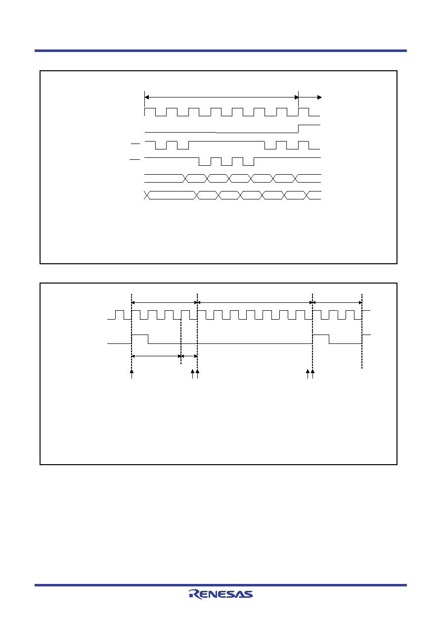
Fig 22. Interrupt sequence
Fig 23. Timing of interrupt request generation, interrupt request bit, and interrupt acceptance
<Notes>
The interrupt request bit may be set to “1” in the following cases.
<When switching external interrupt active edge>
INT0 interrupt edge selection bit
(bit 0 of Interrupt edge selection register (address 3A16))
INT1 interrupt edge selection bit
(bit 1 of Interrupt edge selection register)
If it is not necessary to generate an interrupt synchronized with
these settings, take the following sequence.
(1) Set the corresponding enable bit to “0” (disabled).
(2) Set the interrupt edge selection bit (the active edge switch
bit) or the interrupt source bit.
(3) Set the corresponding interrupt request bit to “0” after one
or more instructions have been executed.
(4) Set the corresponding interrupt enable bit to “1” (enabled).
φ
SYNC
RD
WR
Push onto stack
Vector fetch
Address bus
Data bus
Execute interrupt
routine
PC
S,SPS
S-1,SPS S-2,SPS
BL
BH
AL,AH
Not used
PCH
PCL
PS
AL
AH
SYNC : CPU operation code fetch cycle
(This is an internal signal that cannot be observed from the external unit.)
BL, BH: Vector address of each interrupt
AL, AH: Jump destination address of each interrupt
SPS
: “0016” or “0116”
([SPS] is a page selected by the stack page selection bit of CPU mode register.)
T1
(1) The interrupt request bit for an interrupt request generated during period 1 is set to “1” at timing point IR1.
(2) The interrupt request bit for an interrupt request generated during period 2 is set to “1” at timing point IR1 or IR2.
The timing point at which the bit is set to “1” varies depending on conditions. When two or more interrupt
requests are generated during the period 2, each request bit may be set to “1” at timing point IR1 or IR2
separately.
T1 T2 T3 : Interrupt acceptance timing points
IR1 IR2 : Timings points at which the interrupt request bit is set to “1”.
Note : Period 2 indicates the last
φ cycle during one instruction cycle.
IR1 T2
SYNC
IR2 T3
12
Internal clock
φ
Instruction cycle
Push onto stack
Vector fetch
Instruction cycle
相关PDF资料 |
PDF描述 |
|---|---|
| M37548G1FP | 8-BIT, MROM, 8 MHz, MICROCONTROLLER, PDSO20 |
| M37549G1-XXXFP | 8-BIT, MROM, 8 MHz, MICROCONTROLLER, PDSO24 |
| M37549G3-XXXFP | 8-BIT, MROM, 8 MHz, MICROCONTROLLER, PDSO24 |
| M37560M8-XXXFP | 8-BIT, MROM, 8 MHz, MICROCONTROLLER, PQFP100 |
| M37560MF-XXXGP | 8-BIT, MROM, 8 MHz, MICROCONTROLLER, PQFP100 |
相关代理商/技术参数 |
参数描述 |
|---|---|
| M37548G2-XXXFP | 制造商:RENESAS 制造商全称:Renesas Technology Corp 功能描述:SINGLE-CHIP 8-BIT CMOS MICROCOMPUTER |
| M37548G3FP | 制造商:RENESAS 制造商全称:Renesas Technology Corp 功能描述:SINGLE-CHIP 8-BIT CMOS MICROCOMPUTER |
| M37548G3FP#U0 | 功能描述:MCU 6K ROM 256K 20-SSOP RoHS:是 类别:集成电路 (IC) >> 嵌入式 - 微控制器, 系列:740/38000 标准包装:250 系列:LPC11Uxx 核心处理器:ARM? Cortex?-M0 芯体尺寸:32-位 速度:50MHz 连通性:I²C,Microwire,SPI,SSI,SSP,UART/USART,USB 外围设备:欠压检测/复位,POR,WDT 输入/输出数:40 程序存储器容量:96KB(96K x 8) 程序存储器类型:闪存 EEPROM 大小:4K x 8 RAM 容量:10K x 8 电压 - 电源 (Vcc/Vdd):1.8 V ~ 3.6 V 数据转换器:A/D 8x10b 振荡器型:内部 工作温度:-40°C ~ 85°C 封装/外壳:48-LQFP 包装:托盘 其它名称:568-9587 |
| M37548G3-XXXFP | 制造商:RENESAS 制造商全称:Renesas Technology Corp 功能描述:SINGLE-CHIP 8-BIT CMOS MICROCOMPUTER |
| M37549G1FP | 制造商:RENESAS 制造商全称:Renesas Technology Corp 功能描述:SINGLE-CHIP 8-BIT CMOS MICROCOMPUTER |
发布紧急采购,3分钟左右您将得到回复。