- 您现在的位置:买卖IC网 > PDF目录69014 > M37754M6C-XXXGP 16-BIT, MROM, 40 MHz, MICROCONTROLLER, PQFP100 PDF资料下载
参数资料
| 型号: | M37754M6C-XXXGP |
| 元件分类: | 微控制器/微处理器 |
| 英文描述: | 16-BIT, MROM, 40 MHz, MICROCONTROLLER, PQFP100 |
| 封装: | PLASTIC, QFP-100 |
| 文件页数: | 15/16页 |
| 文件大小: | 267K |
| 代理商: | M37754M6C-XXXGP |
5
MITSUBISHI MICROCOMPUTERS
M37754M6C-XXXGP
M37754M6C-XXXHP
PRELIMINAR
Y
Notice:
This
is not
a final
specification.
Some
parametric
limits
are
subject
to change.
SINGLE-CHIP 16-BIT CMOS MICROCOMPUTER
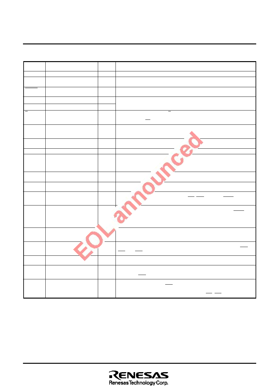
PIN DESCRIPTION (MICROCOMPUTER MODE)
Functions
Input
Output
Input
I/O
Input/
Output
Name
Pin
VCC, VSS
CNVSS
RESET
XIN
XOUT
E
BYTE
(Note)
AVCC,
AVSS
VREF
P00–P07
P10–P17
P20–P23,
P27
P30–P33
P40–P47
P50–P57
P60–P67
P70–P77
P80–P87
P90–P95
Supply 5 V±10 % to VCC and 0 V to VSS.
This pin controls the processor mode. Connect to VSS for single-chip mode or
memory expansion mode. Connect to VCC for microprocessor mode.
This is reset input pin. The microcomputer is reset when supplying “L” level to this
pin.
These are I/O pins of internal clock generating circuit. Connect a ceramic or quartz-
crystal resonator between XIN and XOUT. When an external clock is used, the clock
source should be connected to the XIN pin and the XOUT pin should be left open.
This pin outputs enable signal E, which indicates access state of data bus for
single-chip mode.
This pin outputs RD signal for memory expansion mode or microprocessor mode.
This pin determines whether the external data bus is 8-bit width or 16-bit width for
memory expansion mode or microprocessor mode. The width is 16 bits when “L”
signal inputs and 8 bits when “H” signal inputs.
Power supply for the A-D converter and the D-A converter. Connect AVCC to VCC
and AVSS to VSS externally.
This is reference voltage input pin for the A-D converter and the D-A converter.
In single-chip mode, port P0 is an 8-bit I/O port. This port has an I/O direction
register and each pin can be programmed for input or output. These ports are in
the input mode when reset. Address (A0–A7) is output in memory expansion mode
or microprocessor mode.
In single-chip mode, these pins have the same functions as port P0. Address (A8–
A15) is output in memory expansion mode or microprocessor mode.
In single-chip mode, these pins have the same functions as port P0. Address (A16–
A19, A23) is output in memory expansion mode or microprocessor mode.
In single-chip mode, these pins have the same functions as port P0. In memory
expansion mode or microprocessor mode, WR, BHE , ALE, and HLDA signals are
output.
In single-chip mode, these pins have the same functions as port P0. In memory
expansion mode or microprocessor mode, P40, P41, and P42 become HOLD and
RDY input pins, and clock
φ1 output pin respectively. Functions of other pins are the
same as in single-chip mode. In memory expansion mode, P42 can be pro-
grammed as I/O port.
In addition to having the same functions as port P0 in single-chip mode, these pins
also function as I/O pins for timer A0, timer A1, timer A2, timer A3, output pins for
motor drive waveform, and input pins for key input interrupt.
In addition to having the same functions as port P0 in single-chip mode, these pins
also function as I/O pins for timer A4, input pins for external interrupt input INT0,
INT1, and INT2, and input pins for timer B0, timer B1, and timer B2.
In addition to having the same functions as port P0 in single-chip mode, these pins
also function as input pins for A-D converter.
In addition to having the same functions as port P0 in single-chip mode, these pins
also function as I/O pins for UART0, UART1, output pins for D-A converter, and
input pin for INT4.
In addition to having the same functions as port P0 in single-chip mode, these pins
also function as input pin for INT3, output pins for motor drive waveform.
In memory expansion mode and microprocessor mode, these pins can be
programmed as address (A20–A22) or output pins for CS0–CS4.
Power supply
CNVSS input
Reset input
Clock input
Clock output
Enable output
Bus width select input
Analog supply input
Reference voltage input
I/O port P0
I/O port P1
I/O port P2
I/O port P3
I/O port P4
I/O port P5
I/O port P6
I/O port P7
I/O port P8
I/O port P9
Note: It is impossible to change the input level of the BYTE pin in each bus cycle. In other words, bus width cannot be switched dynamically. Fix the input
level of the BYTE pin to “H” or “L” according to the bus width used.
相关PDF资料 |
PDF描述 |
|---|---|
| M37795STJ | 16-BIT, 8 MHz, MICROCONTROLLER, PQCC84 |
| M37795SJ | 16-BIT, 8 MHz, MICROCONTROLLER, PQCC84 |
| M37903S4CHP | 16-BIT, 26 MHz, MICROCONTROLLER, PQFP100 |
| M37920FCCHP | 16-BIT, FLASH, 20 MHz, MICROCONTROLLER, PQFP100 |
| M37920FCCGP | 16-BIT, FLASH, 20 MHz, MICROCONTROLLER, PQFP100 |
相关代理商/技术参数 |
参数描述 |
|---|---|
| M37754M6C-XXXHP | 制造商:RENESAS 制造商全称:Renesas Technology Corp 功能描述:SINGLE-CHIP 16-BIT CMOS MICROCOMPUTER |
| M37754M8C-XXXGP | 制造商:MITSUBISHI 制造商全称:Mitsubishi Electric Semiconductor 功能描述:SINGLE-CHIP 16BIT CMOS MICROCOMPUTER |
| M37754M8C-XXXHP | 制造商:MITSUBISHI 制造商全称:Mitsubishi Electric Semiconductor 功能描述:SINGLE-CHIP 16BIT CMOS MICROCOMPUTER |
| M37754S4CGP | 制造商:MITSUBISHI 制造商全称:Mitsubishi Electric Semiconductor 功能描述:SINGLE-CHIP 16BIT CMOS MICROCOMPUTER |
| M37754S4CHP | 制造商:RENESAS 制造商全称:Renesas Technology Corp 功能描述:SINGLE-CHIP 16-BIT CMOS MICROCOMPUTER |
发布紧急采购,3分钟左右您将得到回复。