- 您现在的位置:买卖IC网 > PDF目录69014 > M37903S4CHP 16-BIT, 26 MHz, MICROCONTROLLER, PQFP100 PDF资料下载
参数资料
| 型号: | M37903S4CHP |
| 元件分类: | 微控制器/微处理器 |
| 英文描述: | 16-BIT, 26 MHz, MICROCONTROLLER, PQFP100 |
| 封装: | 14 X 14 MM, 0.50 MM PITCH, PLASTIC, LQFP-100 |
| 文件页数: | 7/11页 |
| 文件大小: | 191K |
| 代理商: | M37903S4CHP |
M37903S4CHP
PRELIMINAR
Y
Notice:
This
is not
a final
specification.
Some
parametric
limits
are
subject
to change.
16-BIT CMOS MICROCOMPUTER
MITSUBISHI MICROCOMPUTERS
4
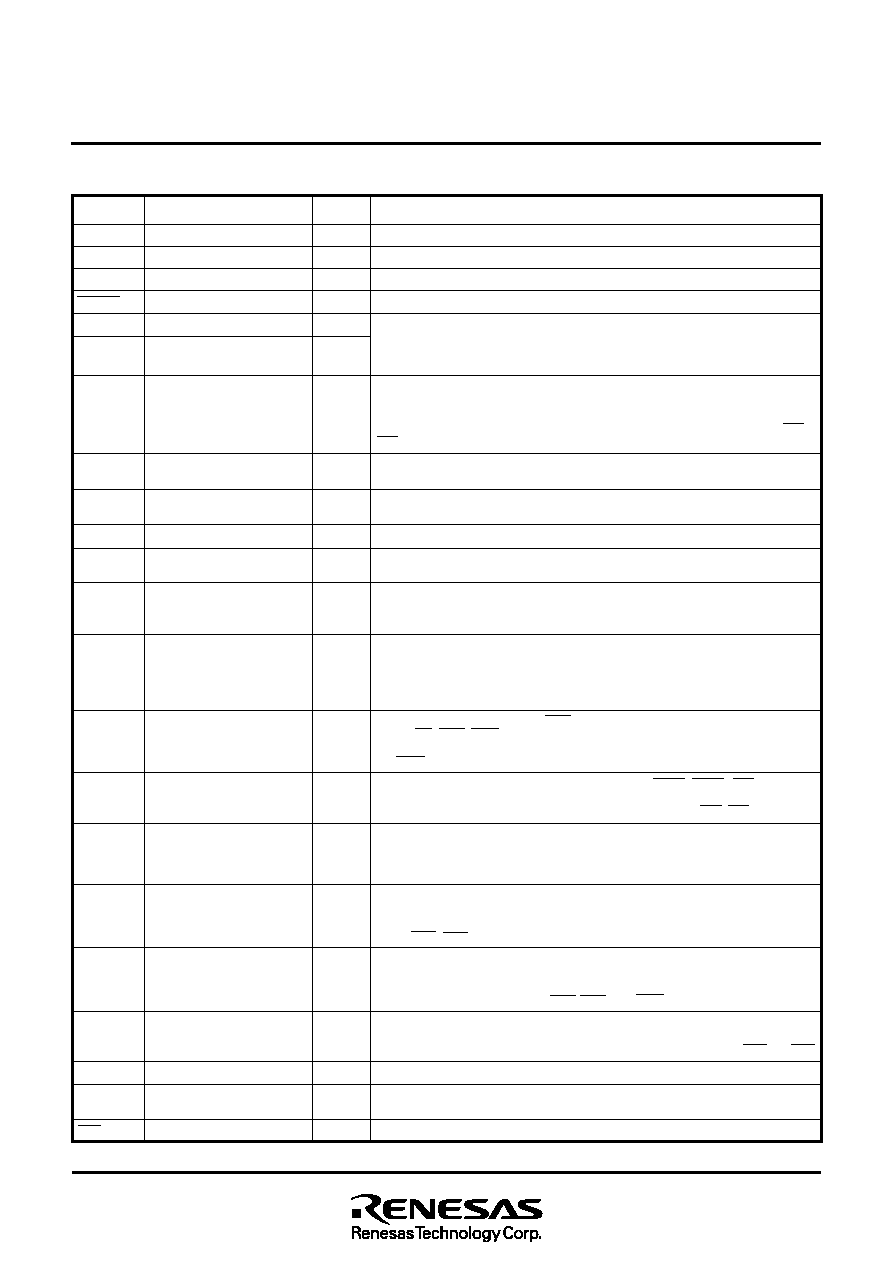
Note: The XIN-input-clock division select bit is used to determine whether the input clock to pin XIN is to be divided or not.
Vcc, Vss
MD0
MD1
RESET
XIN
XOUT
BYTE
CDSEL
AVcc,
AVss
VREF
P00/A16–
P07/A23
P10/D0–
P17/D7
P20/D8–
P27/D15
P30–P33
P40–P47
P50–P57
P60–P67
P70–P77
P80–P87
P100/A0–P107/A7
P110/A8–
P117/A15
NMI
Power supply input
MD0
MD1
Reset input
Clock input
Clock output
External data bus width
select input
Clock division select input
Analog power supply input
Reference voltage input
Address (high-order) output
Data (low-order) I/O
I/O port P2,
Data (high-order) I/O
I/O port P3
I/O port P4
I/O port P5
I/O port P6
I/O port P7
I/O port P8
Address (low-order) output
Address (middle-order)
output
Non-maskable interrupt
—
Input
Output
Input
—
Input
Output
I/O
Output
Input
Apply 5 V±0.5 V to Vcc, and 0 V to Vss.
Connect this pin to VCC.
Connect this pin to Vss.
The microcomputer is reset when VSS-level voltage is applied to this pin.
These are input and output pins of the internal clock generating circuit. Connect a
ceramic or quartz- crystal resonator between the XIN and XOUT pins. When an
external clock is used, the clock source should be connected to the XIN pin, and the
XOUT pin should be left open.
This pin determines whether the external data bus has an 8-bit width or 16-bit width
for the memory expansion mode or microprocessor mode. The width is 16 bits when
VSS-level voltage is input, and 8 bits when VCC-level voltage is applied. When BYTE
= Vss level, by the register setting, the external data bus for each of areas CS1 to
CS3 can have a width of 8 bits.
This pin determines the XIN-input-clock division select bit’s (Note) state at reset and
the input level at pin XIN.
Power supply input pins for the A-D converter and the D-A converter. Connect AVcc
to Vcc, and AVss to Vss externally.
This is the reference voltage input pin for the A-D converter and the D-A converter.
Address (A16–A23) is output. These pins also function as I/O port pins according
to the register setting.
The low-order 8 bits of data (D0–D7) are input/output. When the external data bus
has an 8-bit width, address (LA0–LA7) output and data (D0–D7) input/output can
be performed with the time-sharing method, according to the register setting.
s When 8-bit external data bus is used
Port P2 is an 8-bit I/O port. This port has an I/O direction register, and each pin
can be programmed for input or output. These pins enter the input mode at reset.
s When 16-bit external data bus is used
The high-order 8 bits of data (D8–D15) are input or output.
P30 functions as an input pin of RDY; and P31,P32, P33 function as the output
pins of RD, BLW, BHW, respectively. P30 also functions as an I/O port pin accord-
ing to the register setting. When the external data bus has a width of 8 bits,
the BHW pin functions as an I/O port pin (P33).
P40–P44 function as output or input pins of ALE,
φ1, HLDA, HOLD, CS0, and
P45–P47 as I/O port pins, respectively. According to the register setting, P40–P43
also function as I/O port pins, and P45–P47 as output pins of CS1–CS3.
Port P5 is an 8-bit I/O port. This port has an I/O direction register, and each pin can
be programmed for input or output. These pins enter the input mode at reset.
These pins also function as I/O pins for timers A0–A3, output pins for the real-time
output, and input pins for the key-input interrupt.
Port P6 is an 8-bit I/O port. This port has an I/O direction register, and each pin can
be programmed for input or output. These pins enter the input mode at reset.
These pins also function as I/O pins for timer A4, input pins for external interrupt
inputs INT0–INT2, and input pins for timers B0–B2.
Port P7 is an 8-bit I/O port. This port has an I/O direction register, and each pin
can be programmed for input or output. These pins enter the input mode at reset.
These pins also function as input pins for the A-D converter, output pins for the
D-A converter, and input pins for INT2, INT3, and INT4.
Port P8 is an 8-bit I/O port. This port has an I/O direction register, and each pin
can be programmed for input or output. These pins enter the input mode at reset.
These pins also function as I/O pins for UART0, UART1, and input pins for INT3 and INT4.
Address (A0–A7) is output.
Address (A8–A15) is output. Also, these pins function as I/O port pins according to
the register setting.
This pin is for a non-maskable interrupt.
PIN DESCRIPTION (MICROCOMPUTER MODE)
Functions
Input/
Output
Name
Pin
相关PDF资料 |
PDF描述 |
|---|---|
| M37920FCCHP | 16-BIT, FLASH, 20 MHz, MICROCONTROLLER, PQFP100 |
| M37920FCCGP | 16-BIT, FLASH, 20 MHz, MICROCONTROLLER, PQFP100 |
| M38039MFL-XXXWG | 8-BIT, MROM, 16.8 MHz, MICROCONTROLLER, PBGA64 |
| M38039FFLSP | 8-BIT, FLASH, 16.8 MHz, MICROCONTROLLER, PDIP64 |
| M38039FFLKP | 8-BIT, FLASH, 16.8 MHz, MICROCONTROLLER, PQFP64 |
相关代理商/技术参数 |
参数描述 |
|---|---|
| M37905F8CFP | 制造商:MITSUBISHI 制造商全称:Mitsubishi Electric Semiconductor 功能描述:16-BIT CMOS MICROCOMPUTER |
| M37905F8CSP | 制造商:MITSUBISHI 制造商全称:Mitsubishi Electric Semiconductor 功能描述:16-BIT CMOS MICROCOMPUTER |
| M37905M4C | 制造商:MITSUBISHI 制造商全称:Mitsubishi Electric Semiconductor 功能描述:16 BIT CMOS MICROCOMPUTER |
| M37905M4C-XXXFP | 制造商:MITSUBISHI 制造商全称:Mitsubishi Electric Semiconductor 功能描述:16 BIT CMOS MICROCOMPUTER |
| M37905M4C-XXXSP | 制造商:MITSUBISHI 制造商全称:Mitsubishi Electric Semiconductor 功能描述:16 BIT CMOS MICROCOMPUTER |
发布紧急采购,3分钟左右您将得到回复。