- 您现在的位置:买卖IC网 > PDF目录67763 > M38039MFL-XXXKP 8-BIT, MROM, 16.8 MHz, MICROCONTROLLER, PQFP64 PDF资料下载
参数资料
| 型号: | M38039MFL-XXXKP |
| 元件分类: | 微控制器/微处理器 |
| 英文描述: | 8-BIT, MROM, 16.8 MHz, MICROCONTROLLER, PQFP64 |
| 封装: | 14 X 14 MM, 0.80 MM PITCH, PLASTIC, LQFP-64 |
| 文件页数: | 5/121页 |
| 文件大小: | 2071K |
| 代理商: | M38039MFL-XXXKP |
第1页第2页第3页第4页当前第5页第6页第7页第8页第9页第10页第11页第12页第13页第14页第15页第16页第17页第18页第19页第20页第21页第22页第23页第24页第25页第26页第27页第28页第29页第30页第31页第32页第33页第34页第35页第36页第37页第38页第39页第40页第41页第42页第43页第44页第45页第46页第47页第48页第49页第50页第51页第52页第53页第54页第55页第56页第57页第58页第59页第60页第61页第62页第63页第64页第65页第66页第67页第68页第69页第70页第71页第72页第73页第74页第75页第76页第77页第78页第79页第80页第81页第82页第83页第84页第85页第86页第87页第88页第89页第90页第91页第92页第93页第94页第95页第96页第97页第98页第99页第100页第101页第102页第103页第104页第105页第106页第107页第108页第109页第110页第111页第112页第113页第114页第115页第116页第117页第118页第119页第120页第121页
Rev.1.01
Jan 25, 2008
Page 100 of 117
REJ03B0212-0101
3803 Group (Spec.L)
Notes on Restarting Oscillation
Restarting oscillation
Usually, when the MCU stops the clock oscillation by STP
instruction and the STP instruction has been released by an
external interrupt source, the fixed values of Timer 1 and
Prescaler 12 (Timer 1 = “0116”, Prescaler 12 = “FF16”) are
automatically reloaded in order for the oscillation to stabilize.
The user can inhibit the automatic setting by writing “1” to bit 0
of MISRG (address 001016).
However, by setting this bit to “1”, the previous values, set just
before the STP instruction was executed, will remain in Timer 1
and Prescaler 12. Therefore, you will need to set an appropriate
value to each register, in accordance with the oscillation
stabilizing time, before executing the STP instruction.
<Reason>
Oscillation will restart when an external interrupt is received.
However, internal clock
φ is supplied to the CPU only when
Timer 1 starts to underflow. This ensures time for the clock
oscillation using the ceramic resonators to be stabilized.
Notes on Using Stop Mode
Register setting
Since values of the prescaler 12 and Timer 1 are automatically
reloaded when returning from the stop mode, set them again,
respectively. (When the oscillation stabilizing time set after STP
instruction released bit is “0”)
Clock restoration
After restoration from the stop mode to the normal mode by an
interrupt request, the contents of the CPU mode register previous
to the STP instruction execution are retained. Accordingly, if
both main clock and sub clock were oscillating before execution
of the STP instruction, the oscillation of both clocks is resumed
at restoration.
In the above case, when the main clock side is set as a system
clock, the oscillation stabilizing time for approximately 8,000
cycles of the XIN input is reserved at restoration from the stop
mode. At this time, note that the oscillation on the sub clock side
may not be stabilized even after the lapse of the oscillation
stabilizing time of the main clock side.
Notes on Wait Mode
Clock restoration
If the wait mode is released by a reset when XCIN is set as the
system clock and XIN oscillation is stopped during execution of
the WIT instruction, XCIN oscillation stops, XIN oscillations
starts, and XIN is set as the system clock.
In the above case, the RESET pin should be held at “L” until the
oscillation is stabilized.
Notes on CPU rewrite mode of flash memory version
1. Operation speed
During CPU rewrite mode, set the system clock
φ 4.0 MHz or
less using the main clock division ratio selection bits (bits 6 and
7 of address 003B16).
2. Instructions inhibited against use
The instructions which refer to the internal data of the flash
memory cannot be used during the CPU rewrite mode.
3. Interrupts inhibited against use
The interrupts cannot be used during the CPU rewrite mode
because they refer to the internal data of the flash memory.
4. Watchdog timer
In case of the watchdog timer has been running already, the
internal reset generated by watchdog timer underflow does not
happen, because of watchdog timer is always clearing during
program or erase operation.
5. Reset
Reset is always valid. In case of CNVSS = “H” when reset is
released, boot mode is active. So the program starts from the
address contained in address FFFC16 and FFFD16 in boot ROM
area.
Notes on flash memory version
The CNVSS pin determines the flash memory mode.
Connect the CNVSS pin the shortest possible to the GND pattern
which is supplied to the VSS pin of the microcomputer.
In addition connecting an approximately 5 k
. resistor in series
to the GND could improve noise immunity. In this case as well
as the above mention, connect the pin the shortest possible to the
GND pattern which is supplied to the VSS pin o f the
microcomputer.
Note. When the boot mode or the standard serial I/O mode is used, a
switch of the input level to the CNVSS pin is required.
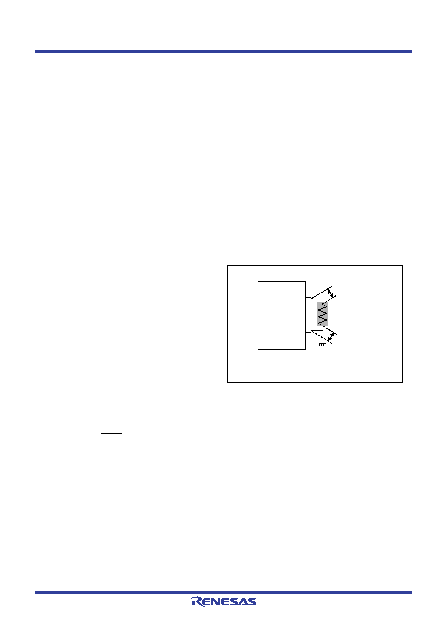
Fig 99. Wiring for the CNVSS
Notes on electric characteristic differences between
mask ROM and flash nemory version MCUs
There are differences in electric characteristics, operation
margin, noise immunity, and noise radiation between Mask
ROM and Flash Memory version MCUs due to the difference in
the manufacturing processes, built-in ROM, and layout pattern
etc. When manufacturing an application system with the Flash
Memory version and then switching to use of the Mask ROM
version, please conduct evaluations equivalent to the system
evaluations conducted for the flash memory version.
DATA REQUIRED FOR MASK ORDERS
The following are necessary when ordering a mask ROM
production:
1. Mask ROM Confirmation Form*
2. Mark Specification Form*
3. Data to be written to ROM, in EPROM form (three identical
copies)
* For the mask ROM confirmation and the mark specifications,
refer to the “Renesas Technology Corp.” Homepage
(http://www.renesas.com/en/rom).
The shortest
CNVSS
VSS
Approx. 5k
The shortest
(Note)
Note: Shows the microcomputer’s pin.
相关PDF资料 |
PDF描述 |
|---|---|
| M38039FFLSP | 8-BIT, FLASH, 16.8 MHz, MICROCONTROLLER, PDIP64 |
| M38039FFLKP | 8-BIT, FLASH, 16.8 MHz, MICROCONTROLLER, PQFP64 |
| M38049FFLWG | 8-BIT, FLASH, 16.8 MHz, MICROCONTROLLER, PBGA64 |
| M38049FFLHP | 8-BIT, FLASH, 16.8 MHz, MICROCONTROLLER, PQFP64 |
| M38049FFLSP | 8-BIT, FLASH, 16.8 MHz, MICROCONTROLLER, PDIP64 |
相关代理商/技术参数 |
参数描述 |
|---|---|
| M38049FFFP#U0 | 制造商:Renesas Electronics Corporation 功能描述: |
| M38049FFLHP#U0 | 制造商:Renesas Electronics Corporation 功能描述: |
| M38049RLSS | 功能描述:DEV EMULATOR CHIP RAM 2KB 64SDIP RoHS:否 类别:编程器,开发系统 >> 内电路编程器、仿真器以及调试器 系列:- 产品变化通告:Development Systems Discontinuation 19/Jul/2010 标准包装:1 系列:* 类型:* 适用于相关产品:* 所含物品:* |
| M3806 | 功能描述:电缆固定件和配件 LTSCG 625 BLACK RoHS:否 制造商:Heyco 类型:Cable Grips, Liquid Tight 材料:Nylon 颜色:Black 安装方法:Cable 最大光束直径:11.4 mm 抗拉强度: |
| M3806 BK001 | 制造商:Alpha Wire Company 功能描述:CBL 8COND 18AWG BLK 1000' |
发布紧急采购,3分钟左右您将得到回复。