- 您现在的位置:买卖IC网 > PDF目录80361 > M38047M8-XXXSP 8-BIT, MROM, 8.4 MHz, MICROCONTROLLER, PDIP64 PDF资料下载
参数资料
| 型号: | M38047M8-XXXSP |
| 元件分类: | 微控制器/微处理器 |
| 英文描述: | 8-BIT, MROM, 8.4 MHz, MICROCONTROLLER, PDIP64 |
| 封装: | 0.750 INCH, 1.78 MM PITCH, PLASTIC, SDIP-64 |
| 文件页数: | 17/138页 |
| 文件大小: | 1887K |
| 代理商: | M38047M8-XXXSP |
第1页第2页第3页第4页第5页第6页第7页第8页第9页第10页第11页第12页第13页第14页第15页第16页当前第17页第18页第19页第20页第21页第22页第23页第24页第25页第26页第27页第28页第29页第30页第31页第32页第33页第34页第35页第36页第37页第38页第39页第40页第41页第42页第43页第44页第45页第46页第47页第48页第49页第50页第51页第52页第53页第54页第55页第56页第57页第58页第59页第60页第61页第62页第63页第64页第65页第66页第67页第68页第69页第70页第71页第72页第73页第74页第75页第76页第77页第78页第79页第80页第81页第82页第83页第84页第85页第86页第87页第88页第89页第90页第91页第92页第93页第94页第95页第96页第97页第98页第99页第100页第101页第102页第103页第104页第105页第106页第107页第108页第109页第110页第111页第112页第113页第114页第115页第116页第117页第118页第119页第120页第121页第122页第123页第124页第125页第126页第127页第128页第129页第130页第131页第132页第133页第134页第135页第136页第137页第138页
Rev.4.01
Nov 14, 2003
page 111 of 136
3803/3804 Group
q CPU reprogramming mode operation procedure
The operation procedure in CPU reprogramming mode is de-
scribed below.
< Beginning procedure >
Apply 0 V to the CNVss/VPP pin for reset release.
Set the CPU mode register (see Figure 103).
After CPU reprogramming mode control program is transferred to
internal RAM, jump to this control program on RAM. (The follow-
ing operations are controlled by this control program).
Set “1" to the CPU reprogramming mode select bit.
Apply VPPH to the CNVSS/VPP pin.
Wait till CNVSS/VPP pin becomes 12V.
Read the CPU reprogramming mode monitor flag to confirm
whether the CPU reprogramming mode is valid.
The operation of the flash memory is executed by software-com-
mand-writing to the flash command register .
Note: The following are necessary other than this:
Control for data which is input from the external (serial I/O
etc.) and to be programmed to the flash memory
Initial setting for ports etc.
Writing to the watchdog timer
< Release procedure >
Apply 0 V to the CNVSS/VPP pin.
Wait till CNVSS/VPP pin becomes 0 V.
Set the CPU reprogramming mode select bit to “0.”
Each software command is explained as follows.
q Read command
When “0016" is written to the flash command register, the 3803/
3804 group enters the read mode. The contents of the corre-
sponding address can be read by reading the flash memory (For
instance, with the LDA instruction etc.) under this condition.
The read mode is maintained until another command code is written
to the flash command register. Accordingly, after setting the read
mode once, the contents of the flash memory can continuously be
read.
After reset and after the reset command is executed, the read
mode is set.
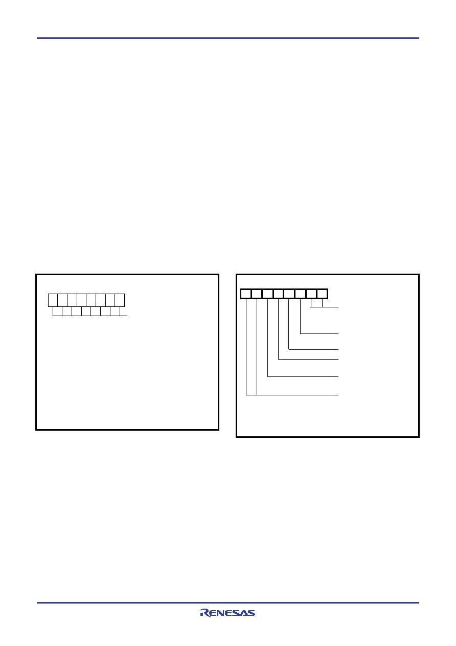
Fig. 102 Flash command register bit configuration
Fig. 103 CPU mode register bit configuration in CPU rewriting
mode
Writing of software command
<Command code>
“0016”
“4016”
“C016”
“2016” + “2016”
“A016”
“FF16” + “FF16”
<Software command name>
Read command
Program command
Program verify command
Erase command
Erase verify command
Reset command
Note: The flash command register is write-only register.
Flash command register
(FCMD : address 0FFF16)
76
5
4
3
2
1
0
Processor mode bits
b1 b0
0
0 : Single-chip mode
0
1 : Not available
1
X : Not available
Port XC switch bit
0 : I/O port function (stop oscillating)
1 : XCIN–XCOUT oscillating function
Main clock (XIN–XOUT) stop bit
0 : Oscillating
1 : Stopped
Main clock division ratio selection bits
b7 b6
0
0 :
φ = f(XIN)/2 (high-speed mode)
0
1 :
φ = f(XIN)/8 (middle-speed mode)
1
0 :
φ = f(XCIN)/2 (low-speed mode)
1
1 : Not available
00
1
CPU mode register
(CPUM : address 003B16)
b7
b0
Stack page selection bit
0 : 0 page
1 : 1 page
Fix this bit to “1”.
相关PDF资料 |
PDF描述 |
|---|---|
| M38234G4-XXXHP | 8-BIT, MROM, 10 MHz, MICROCONTROLLER, PQFP80 |
| M102P0200.0000DK | 200 MHz, OTHER CLOCK GENERATOR, MDIP24 |
| M30800SFP | 16-BIT, MROM, 20 MHz, MICROCONTROLLER, PQFP100 |
| M38C24M4-XXXFP | 8-BIT, MROM, 4 MHz, MICROCONTROLLER, PQFP64 |
| MAXQ610X-0000+ | 16-BIT, FLASH, 12 MHz, RISC MICROCONTROLLER, UUC |
相关代理商/技术参数 |
参数描述 |
|---|---|
| M38049FFFP#U0 | 制造商:Renesas Electronics Corporation 功能描述: |
| M38049FFLHP#U0 | 制造商:Renesas Electronics Corporation 功能描述: |
| M38049RLSS | 功能描述:DEV EMULATOR CHIP RAM 2KB 64SDIP RoHS:否 类别:编程器,开发系统 >> 内电路编程器、仿真器以及调试器 系列:- 产品变化通告:Development Systems Discontinuation 19/Jul/2010 标准包装:1 系列:* 类型:* 适用于相关产品:* 所含物品:* |
| M3806 | 功能描述:电缆固定件和配件 LTSCG 625 BLACK RoHS:否 制造商:Heyco 类型:Cable Grips, Liquid Tight 材料:Nylon 颜色:Black 安装方法:Cable 最大光束直径:11.4 mm 抗拉强度: |
| M3806 BK001 | 制造商:Alpha Wire Company 功能描述:CBL 8COND 18AWG BLK 1000' |
发布紧急采购,3分钟左右您将得到回复。