- 您现在的位置:买卖IC网 > PDF目录67763 > M38049FFLSP 8-BIT, FLASH, 16.8 MHz, MICROCONTROLLER, PDIP64 PDF资料下载
参数资料
| 型号: | M38049FFLSP |
| 元件分类: | 微控制器/微处理器 |
| 英文描述: | 8-BIT, FLASH, 16.8 MHz, MICROCONTROLLER, PDIP64 |
| 封装: | 17 X 56.40 MM, 1.78 MM HEIGHT, PLASTIC, SDIP-64 |
| 文件页数: | 10/129页 |
| 文件大小: | 1721K |
| 代理商: | M38049FFLSP |
第1页第2页第3页第4页第5页第6页第7页第8页第9页当前第10页第11页第12页第13页第14页第15页第16页第17页第18页第19页第20页第21页第22页第23页第24页第25页第26页第27页第28页第29页第30页第31页第32页第33页第34页第35页第36页第37页第38页第39页第40页第41页第42页第43页第44页第45页第46页第47页第48页第49页第50页第51页第52页第53页第54页第55页第56页第57页第58页第59页第60页第61页第62页第63页第64页第65页第66页第67页第68页第69页第70页第71页第72页第73页第74页第75页第76页第77页第78页第79页第80页第81页第82页第83页第84页第85页第86页第87页第88页第89页第90页第91页第92页第93页第94页第95页第96页第97页第98页第99页第100页第101页第102页第103页第104页第105页第106页第107页第108页第109页第110页第111页第112页第113页第114页第115页第116页第117页第118页第119页第120页第121页第122页第123页第124页第125页第126页第127页第128页第129页
Rev.1.00
Oct 27, 2008
Page 107 of 128
REJ03B0266-0100
3804 Group (Spec.L)
Countermeasures against noise
(1) Shortest wiring length
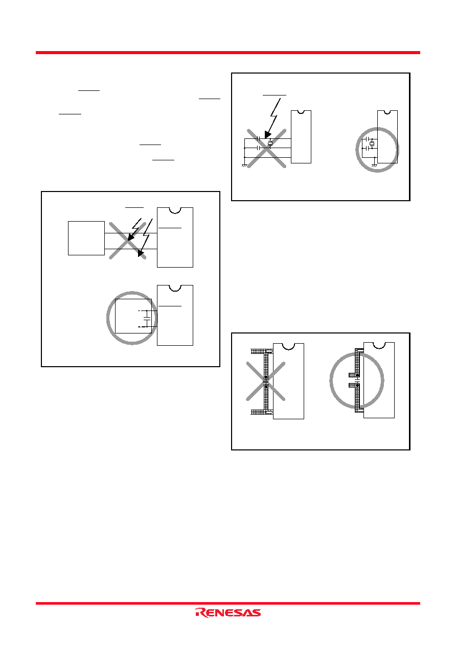
1. Wiring for RESET pin
Make the length of wiring which is connected to the RESET
pin as short as possible. Especially, connect a capacitor across
the RESET pin and the VSS pin with the shortest possible
wiring (within 20mm).
<Reason>
The width of a pulse input into the RESET pin is determined by
the timing necessary conditions. If noise having a shorter pulse
width than the standard is input to the RESET pin, the reset is
released before the internal state of the microcomputer is com-
pletely initialized. This may cause a program runaway.
Fig. 104 Wiring for the RESET pin
2. Wiring for clock input/output pins
Make the length of wiring which is connected to clock I/O
pins as short as possible.
Make the length of wiring (within 20 mm) across the
grounding lead of a capacitor which is connected to an
oscillator and the VSS pin of a microcomputer as short as
possible.
Separate the VSS pattern only for oscillation from other VSS
patterns.
<Reason>
If noise enters clock I/O pins, clock waveforms may be
deformed. This may cause a program failure or program
runaway. Also, if a potential difference is caused by the noise
between the VSS level of a microcomputer and the VSS level of
an oscillator, the correct clock will not be input in the
microcomputer.
Fig. 105 Wiring for clock I/O pins
(2) Connection of bypass capacitor across VSS line and VCC line
In order to stabilize the system operation and avoid the latch-up,
connect an approximately 0.1
μF bypass capacitor across the VSS
line and the VCC line as follows:
Connect a bypass capacitor across the VSS pin and the VCC pin
at equal length.
Connect a bypass capacitor across the VSS pin and the VCC pin
with the shortest possible wiring.
Use lines with a larger diameter than other signal lines for VSS
line and VCC line.
Connect the power source wiring via a bypass capacitor to the
VSS pin and the VCC pin.
Fig. 106 Bypass capacitor across the VSS line and the
VCC line
RESET
Reset
circuit
Noise
VSS
N.G.
Reset
circuit
VSS
RESET
VSS
O.K.
Noise
XIN
XOUT
VSS
N.G.
XIN
XOUT
VSS
O.K.
VSS
VCC
VSS
VCC
N.G.
O.K.
相关PDF资料 |
PDF描述 |
|---|---|
| M38112E4SS | 8-BIT, UVPROM, 4.19 MHz, MICROCONTROLLER, CDIP64 |
| M38112E4-XXXFP | 8-BIT, OTPROM, 4.19 MHz, MICROCONTROLLER, PQFP64 |
| M38112E4-XXXSP | 8-BIT, OTPROM, 4.19 MHz, MICROCONTROLLER, PDIP64 |
| M38112E4FS | 8-BIT, UVPROM, 4.19 MHz, MICROCONTROLLER, CQCC64 |
| M38204RFS | 8-BIT, 8 MHz, MICROCONTROLLER, PQFP80 |
相关代理商/技术参数 |
参数描述 |
|---|---|
| M38049RLSS | 功能描述:DEV EMULATOR CHIP RAM 2KB 64SDIP RoHS:否 类别:编程器,开发系统 >> 内电路编程器、仿真器以及调试器 系列:- 产品变化通告:Development Systems Discontinuation 19/Jul/2010 标准包装:1 系列:* 类型:* 适用于相关产品:* 所含物品:* |
| M3806 | 功能描述:电缆固定件和配件 LTSCG 625 BLACK RoHS:否 制造商:Heyco 类型:Cable Grips, Liquid Tight 材料:Nylon 颜色:Black 安装方法:Cable 最大光束直径:11.4 mm 抗拉强度: |
| M3806 BK001 | 制造商:Alpha Wire Company 功能描述:CBL 8COND 18AWG BLK 1000' |
| M3806 BK002 | 制造商:Alpha Wire Company 功能描述:CBL 8COND 18AWG BLK 500' |
| M3806 BK005 | 制造商:Alpha Wire Company 功能描述:CBL 8COND 18AWG BLK 100' |
发布紧急采购,3分钟左右您将得到回复。