- 您现在的位置:买卖IC网 > PDF目录80395 > M38235G6FP 8-BIT, MROM, 10 MHz, MICROCONTROLLER, PQFP80 PDF资料下载
参数资料
| 型号: | M38235G6FP |
| 元件分类: | 微控制器/微处理器 |
| 英文描述: | 8-BIT, MROM, 10 MHz, MICROCONTROLLER, PQFP80 |
| 封装: | 14 X 20 MM, 0.80 MM PITCH, PLASTIC, QFP-80 |
| 文件页数: | 26/64页 |
| 文件大小: | 922K |
| 代理商: | M38235G6FP |
第1页第2页第3页第4页第5页第6页第7页第8页第9页第10页第11页第12页第13页第14页第15页第16页第17页第18页第19页第20页第21页第22页第23页第24页第25页当前第26页第27页第28页第29页第30页第31页第32页第33页第34页第35页第36页第37页第38页第39页第40页第41页第42页第43页第44页第45页第46页第47页第48页第49页第50页第51页第52页第53页第54页第55页第56页第57页第58页第59页第60页第61页第62页第63页第64页
Rev.2.02
Jun 19, 2007
page 30 of 73
REJ03B0146-0202
3823 Group
Timer X
Timer X is a 16-bit timer that can be selected in one of four modes
and can be controlled the timer X write and the real time port by
setting the timer X mode register.
(1) Timer Mode
The timer counts f(XIN)/16 (or f(SUB)/16 in low-speed mode).
f(SUB) is the source oscillation frequency in low-speed mode.
f(SUB) shows the oscillation frequency of XCIN or the on-chip os-
cillator. Internal clock φ is f(XCIN)/2 in the low-speed mode.
(2) Pulse Output Mode
Each time the timer underflows, a signal output from the CNTR0
pin is inverted. Except for this, the operation in pulse output mode
is the same as in timer mode. When using a timer in this mode,
set the corresponding port P54 direction register to output mode.
(3) Event Counter Mode
The timer counts signals input through the CNTR0 pin.
Except for this, the operation in event counter mode is the same
as in timer mode. When using a timer in this mode, set the corre-
sponding port P54 direction register to input mode.
(4) Pulse Width Measurement Mode
The count source is f(XIN)/16 (or f(SUB)/16 in low-speed mode). If
CNTR0 active edge switch bit is “0”, the timer counts while the in-
put signal of CNTR0 pin is at “H”. If it is “1”, the timer counts while
the input signal of CNTR0 pin is at “L”. When using a timer in this
mode, set the corresponding port P54 direction register to input
mode.
●Timer X write control
If the timer X write control bit is “0”, when the value is written in the
address of timer X, the value is loaded in the timer X and the latch
at the same time.
If the timer X write control bit is “1”, when the value is written in the
address of timer X, the value is loaded only in the latch. The value
in the latch is loaded in timer X after timer X underflows.
If the value is written in latch only, when writing in the timer latch at
the timer underflow, the value is set in the timer and the latch at
one time. Additionally, unexpected value may be set in the high-or-
der counter when the writing in high-order latch and the underflow
of timer X are performed at the same timing.
●Real time port control
While the real time port function is valid, data for the real time port
are output from ports P52 and P53 each time the timer X
underflows. (However, after rewriting a data for real time port, if
the real time port control bit is changed from “0” to “1”, data are
output independent of the timer X operation.) If the data for the
real time port is changed while the real time port function is valid,
the changed data are output at the next underflow of timer X.
Before using this function, set the corresponding port direction
registers to output mode.
■Note on CNTR0 interrupt active edge
selection
CNTR0 interrupt active edge depends on the CNTR0 active edge
switch bit.
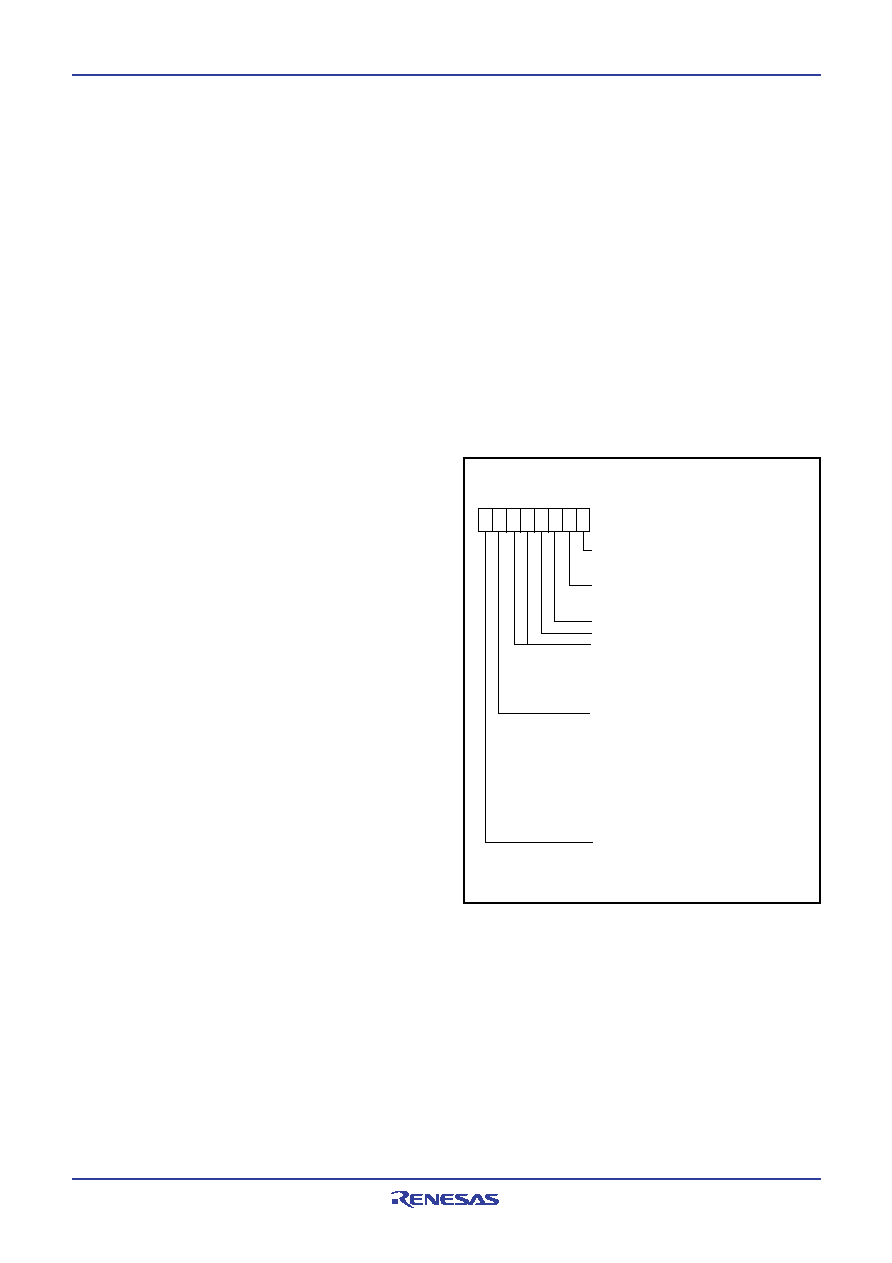
Fig. 23 Structure of timer X mode register
Timer X mode register
(TXM : address 002716)
Timer X write control bit
0 : Write value in latch and counter
1 : Write value in latch only
Real time port control bit
0 : Real time port function invalid
1 : Real time port function valid
P52 data for real time port
P53 data for real time port
Timer X operating mode bits
b5 b4
0
0 : Timer mode
0
1 : Pulse output mode
1
0 : Event counter mode
1
1 : Pulse width measurement mode
CNTR0 active edge switch bit
0 : Count at rising edge in event counter mode
Start from “H” output in pulse output mode
Measure “H” pulse width in pulse width
measurement mode
Falling edge active for CNTR0 interrupt
1 : Count at falling edge in event counter mode
Start from “L” output in pulse output mode
Measure “L” pulse width in pulse width
measurement mode
Rising edge active for CNTR0 interrupt
Timer X stop control bit
0 : Count start
1 : Count stop
b7
b0
相关PDF资料 |
PDF描述 |
|---|---|
| M102E1000.0000AK | 1000 MHz, OTHER CLOCK GENERATOR, MDIP24 |
| M32192F8TWG | 32-BIT, FLASH, 160 MHz, RISC MICROCONTROLLER, PBGA224 |
| M37532M4-XXXGP | 8-BIT, MROM, 6 MHz, MICROCONTROLLER, PQFP32 |
| M37542F8TGP | 8-BIT, FLASH, 8 MHz, MICROCONTROLLER, PQFP32 |
| MB95F106AJWPFM | 8-BIT, FLASH, 16.25 MHz, MICROCONTROLLER, PQFP64 |
相关代理商/技术参数 |
参数描述 |
|---|---|
| M38235G6FP#U0 | 功能描述:MCU 2/5V 24K 80-QFP QZ-ROM RoHS:是 类别:集成电路 (IC) >> 嵌入式 - 微控制器, 系列:740/38000 标准包装:250 系列:80C 核心处理器:8051 芯体尺寸:8-位 速度:16MHz 连通性:EBI/EMI,I²C,UART/USART 外围设备:POR,PWM,WDT 输入/输出数:40 程序存储器容量:- 程序存储器类型:ROMless EEPROM 大小:- RAM 容量:256 x 8 电压 - 电源 (Vcc/Vdd):4.5 V ~ 5.5 V 数据转换器:A/D 8x10b 振荡器型:内部 工作温度:-40°C ~ 85°C 封装/外壳:68-LCC(J 形引线) 包装:带卷 (TR) |
| M38235G6HP#U0 | 功能描述:MCU 2/5V 24K 80-LQFP QZ-ROM RoHS:是 类别:集成电路 (IC) >> 嵌入式 - 微控制器, 系列:740/38000 标准包装:250 系列:80C 核心处理器:8051 芯体尺寸:8-位 速度:16MHz 连通性:EBI/EMI,I²C,UART/USART 外围设备:POR,PWM,WDT 输入/输出数:40 程序存储器容量:- 程序存储器类型:ROMless EEPROM 大小:- RAM 容量:256 x 8 电压 - 电源 (Vcc/Vdd):4.5 V ~ 5.5 V 数据转换器:A/D 8x10b 振荡器型:内部 工作温度:-40°C ~ 85°C 封装/外壳:68-LCC(J 形引线) 包装:带卷 (TR) |
| M38238G8FP#U0 | 功能描述:MCU 2/5V 32K 80-QFP QZ-ROM RoHS:是 类别:集成电路 (IC) >> 嵌入式 - 微控制器, 系列:740/38000 标准包装:250 系列:80C 核心处理器:8051 芯体尺寸:8-位 速度:16MHz 连通性:EBI/EMI,I²C,UART/USART 外围设备:POR,PWM,WDT 输入/输出数:40 程序存储器容量:- 程序存储器类型:ROMless EEPROM 大小:- RAM 容量:256 x 8 电压 - 电源 (Vcc/Vdd):4.5 V ~ 5.5 V 数据转换器:A/D 8x10b 振荡器型:内部 工作温度:-40°C ~ 85°C 封装/外壳:68-LCC(J 形引线) 包装:带卷 (TR) |
| M38238G8HP#U0 | 功能描述:MCU 2/5V 32K 80-LQFP QZ-ROM RoHS:是 类别:集成电路 (IC) >> 嵌入式 - 微控制器, 系列:740/38000 标准包装:250 系列:80C 核心处理器:8051 芯体尺寸:8-位 速度:16MHz 连通性:EBI/EMI,I²C,UART/USART 外围设备:POR,PWM,WDT 输入/输出数:40 程序存储器容量:- 程序存储器类型:ROMless EEPROM 大小:- RAM 容量:256 x 8 电压 - 电源 (Vcc/Vdd):4.5 V ~ 5.5 V 数据转换器:A/D 8x10b 振荡器型:内部 工作温度:-40°C ~ 85°C 封装/外壳:68-LCC(J 形引线) 包装:带卷 (TR) |
| M38239GCFP#U0 | 功能描述:MCU 2/5V 48K 80-QFP QZ-ROM RoHS:是 类别:集成电路 (IC) >> 嵌入式 - 微控制器, 系列:740/38000 标准包装:250 系列:80C 核心处理器:8051 芯体尺寸:8-位 速度:16MHz 连通性:EBI/EMI,I²C,UART/USART 外围设备:POR,PWM,WDT 输入/输出数:40 程序存储器容量:- 程序存储器类型:ROMless EEPROM 大小:- RAM 容量:256 x 8 电压 - 电源 (Vcc/Vdd):4.5 V ~ 5.5 V 数据转换器:A/D 8x10b 振荡器型:内部 工作温度:-40°C ~ 85°C 封装/外壳:68-LCC(J 形引线) 包装:带卷 (TR) |
发布紧急采购,3分钟左右您将得到回复。