- 您现在的位置:买卖IC网 > PDF目录45046 > M38503M2H-XXXFP 8-BIT, MROM, 8 MHz, MICROCONTROLLER, PDSO42 PDF资料下载
参数资料
| 型号: | M38503M2H-XXXFP |
| 元件分类: | 微控制器/微处理器 |
| 英文描述: | 8-BIT, MROM, 8 MHz, MICROCONTROLLER, PDSO42 |
| 封装: | 0.450 INCH, 0.80 MM PITCH, PLASTIC, SSOP-42 |
| 文件页数: | 36/103页 |
| 文件大小: | 1275K |
| 代理商: | M38503M2H-XXXFP |
第1页第2页第3页第4页第5页第6页第7页第8页第9页第10页第11页第12页第13页第14页第15页第16页第17页第18页第19页第20页第21页第22页第23页第24页第25页第26页第27页第28页第29页第30页第31页第32页第33页第34页第35页当前第36页第37页第38页第39页第40页第41页第42页第43页第44页第45页第46页第47页第48页第49页第50页第51页第52页第53页第54页第55页第56页第57页第58页第59页第60页第61页第62页第63页第64页第65页第66页第67页第68页第69页第70页第71页第72页第73页第74页第75页第76页第77页第78页第79页第80页第81页第82页第83页第84页第85页第86页第87页第88页第89页第90页第91页第92页第93页第94页第95页第96页第97页第98页第99页第100页第101页第102页第103页
Rev.3.01
2003.06.20
page 36 of 97
3850 Group (Spec.H/A)
qSERIAL I/O2
The serial I/O2 can be operated only as the clock synchronous type.
As a synchronous clock for serial transfer, either internal clock or
external clock can be selected by the serial I/O2 synchronous clock
selection bit (b6) of serial I/O2 control register 1.
The internal clock incorporates a dedicated divider and permits se-
lecting 6 types of clock by the internal synchronous clock selection
bits (b2, b1, b0) of serial I/O2 control register 1.
Regarding SOUT2 and SCLK2 being output pins, either CMOS output
format or N-channel open-drain output format can be selected by the
P01/SOUT2, P02/SCLK2 P-channel output disable bit (b7) of
serial I/O2 control register 1.
When the internal clock has been selected, a transfer starts by a
write signal to the serial I/O2 register (address 001716). After comple-
tion of data transfer, the level of the SOUT2 pin goes to high imped-
ance automatically but bit 7 of the serial I/O2 control register 2 is not
set to “1” automatically.
When the external clock has been selected, the contents of the serial
I/O2 register is continuously sifted while transfer clocks are input.
Accordingly, control the clock externally. Note that the SOUT2 pin does
not go to high impedance after completion of data transfer.
To cause the SOUT2 pin to go to high impedance in the case where
the external clock is selected, set bit 7 of the serial I/O2 control reg-
ister 2 to “1” when SCLK2 is “H” after completion of data transfer. After
the next data transfer is started (the transfer clock falls), bit 7 of the
serial I/O2 control register 2 is set to “0” and the SOUT2 pin is put into
the active state.
Regardless of the internal clock to external clock, the interrupt re-
quest bit is set after the number of bits (1 to 8 bits) selected by the
optional transfer bit is transferred. In case of a fractional number of
bits less than 8 bits as the last data, the received data to be stored in
the serial I/O2 register becomes a fractional number of bits close to
MSB if the transfer direction selection bit of serial I/O2 control regis-
ter 1 is LSB first, or a fractional number of bits close to LSB if the
transfer direction selection bit is MSB first. For the remaining bits, the
previously received data is shifted.
At transmit operation using the clock synchronous serial I/O, the SCMP2
signal can be output by comparing the state of the transmit pin SOUT2
with the state of the receive pin SIN2 in synchronization with a rise of
the transfer clock. If the output level of the SOUT2 pin is equal to the
input level to the SIN2 pin, “L” is output from the SCMP2 pin. If not, “H”
is output. At this time, an INT2 interrupt request can also be gener-
ated. Select a valid edge by bit 2 of the interrupt edge selection reg-
ister (address 003A16).
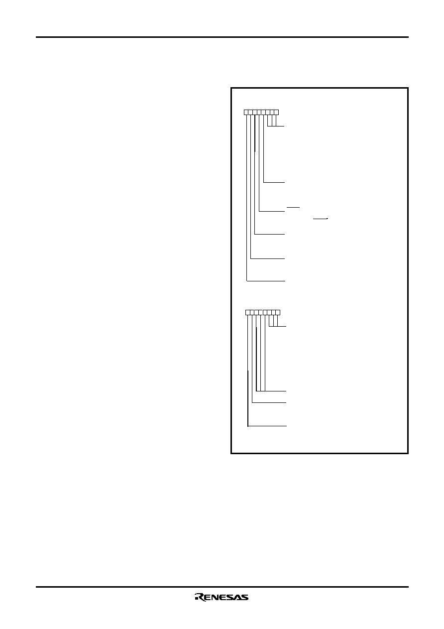
[Serial I/O2 Control Registers 1, 2 (SIO2CON1 /
SIO2CON2)] 001516, 001616
The serial I/O2 control registers 1 and 2 are containing various se-
lection bits for serial I/O2 control as shown in Figure 31.
Fig. 31 Structure of Serial I/O2 control registers 1, 2
Serial I/O2 control register 1
(SIO2CON1 : address 001516)
Serial I/O2 control register 2
(SIO2CON2 : address 001616)
b7
b0
Optional transfer bits
b2 b1 b0
0 0 0: 1 bit
0 0 1: 2 bit
0 1 0: 3 bit
0 1 1: 4 bit
1 0 0: 5 bit
1 0 1: 6 bit
1 1 0: 7 bit
1 1 1: 8 bit
Not used ( returns "0" when read)
Serial I/O2 I/O comparison signal control bit
0: P43 I/O
1: SCMP2 output
SOUT2 pin control bit (P01)
0: Output active
1: Output high-impedance
Internal synchronous clock selection bits
b2 b1 b0
0 0 0: f(XIN)/8 (f(XCIN)/8 in low-speed mode)
0 0 1: f(XIN)/16 (f(XCIN)/16 in low-speed mode)
0 1 0: f(XIN)/32 (f(XCIN)/32 in low-speed mode)
0 1 1: f(XIN)/64 (f(XCIN)/64 in low-speed mode)
1 1 0: f(XIN)/128 f(XCIN)/128 in low-speed mode)
1 1 1: f(XIN)/256 (f(XCIN)/256 in low-speed mode)
Serial I/O2 port selection bit
0: I/O port
1: SOUT2,SCLK2 output pin
SRDY2 output enable bit
0: P03 pin is normal I/O pin
1: P03 pin is SRDY2 output pin
Transfer direction selection bit
0: LSB first
1: MSB first
Serial I/O2 synchronous clock selection bit
0: External clock
1: Internal clock
P01/SOUT2 ,P02/SCLK2 P-channel output disable bit
0: CMOS output (in output mode)
1: N-channel open-drain output (in output mode )
b7
b0
相关PDF资料 |
PDF描述 |
|---|---|
| M38507F8FP | 8-BIT, MROM, 8 MHz, MICROCONTROLLER, PDSO42 |
| M38507M8-XXXSP | 8-BIT, MROM, 8 MHz, MICROCONTROLLER, PDIP42 |
| M38504E6FP | 8-BIT, OTPROM, 8 MHz, MICROCONTROLLER, PDSO42 |
| M38503M4A-XXXSP | 8-BIT, MROM, 12.5 MHz, MICROCONTROLLER, PDIP42 |
| M38503M2A-XXXSP | 8-BIT, MROM, 12.5 MHz, MICROCONTROLLER, PDIP42 |
相关代理商/技术参数 |
参数描述 |
|---|---|
| M38503M4A-210SP | 制造商:Renesas Electronics Corporation 功能描述: |
| M38504E6FP | 制造商:Renesas Electronics Corporation 功能描述:MCU 3/5V 24K 42-SSOP - Trays |
| M38504E6FP#U0 | 功能描述:MCU 4.0/5.5V 24K PB-FREE 42-SSOP RoHS:是 类别:集成电路 (IC) >> 嵌入式 - 微控制器, 系列:740/38000 产品培训模块:CAN Basics Part-1 CAN Basics Part-2 Electromagnetic Noise Reduction Techniques Part 1 M16C Product Overview Part 1 M16C Product Overview Part 2 标准包装:1 系列:M16C™ M32C/80/87 核心处理器:M32C/80 芯体尺寸:16/32-位 速度:32MHz 连通性:EBI/EMI,I²C,IEBus,IrDA,SIO,UART/USART 外围设备:DMA,POR,PWM,WDT 输入/输出数:121 程序存储器容量:384KB(384K x 8) 程序存储器类型:闪存 EEPROM 大小:- RAM 容量:24K x 8 电压 - 电源 (Vcc/Vdd):3 V ~ 5.5 V 数据转换器:A/D 34x10b,D/A 2x8b 振荡器型:内部 工作温度:-20°C ~ 85°C 封装/外壳:144-LQFP 包装:托盘 产品目录页面:749 (CN2011-ZH PDF) 配用:R0K330879S001BE-ND - KIT DEV RSK M32C/87 |
| M38504M6202F | 制造商:Panasonic Industrial Company 功能描述:SUB ONLY IC |
| M38504M6211F | 制造商:Panasonic Industrial Company 功能描述:IC SUB FOR P-M38504M6202F |
发布紧急采购,3分钟左右您将得到回复。