- 您现在的位置:买卖IC网 > PDF目录201872 > M38D28G8-XXXHP 8-BIT, FLASH, 6.25 MHz, MICROCONTROLLER, PQFP64 PDF资料下载
参数资料
| 型号: | M38D28G8-XXXHP |
| 元件分类: | 微控制器/微处理器 |
| 英文描述: | 8-BIT, FLASH, 6.25 MHz, MICROCONTROLLER, PQFP64 |
| 封装: | 10X 10 MM, 0.50 MM PITCH, PLASTIC, LQFP-64 |
| 文件页数: | 13/136页 |
| 文件大小: | 2856K |
| 代理商: | M38D28G8-XXXHP |
第1页第2页第3页第4页第5页第6页第7页第8页第9页第10页第11页第12页当前第13页第14页第15页第16页第17页第18页第19页第20页第21页第22页第23页第24页第25页第26页第27页第28页第29页第30页第31页第32页第33页第34页第35页第36页第37页第38页第39页第40页第41页第42页第43页第44页第45页第46页第47页第48页第49页第50页第51页第52页第53页第54页第55页第56页第57页第58页第59页第60页第61页第62页第63页第64页第65页第66页第67页第68页第69页第70页第71页第72页第73页第74页第75页第76页第77页第78页第79页第80页第81页第82页第83页第84页第85页第86页第87页第88页第89页第90页第91页第92页第93页第94页第95页第96页第97页第98页第99页第100页第101页第102页第103页第104页第105页第106页第107页第108页第109页第110页第111页第112页第113页第114页第115页第116页第117页第118页第119页第120页第121页第122页第123页第124页第125页第126页第127页第128页第129页第130页第131页第132页第133页第134页第135页第136页
Rev.3.02
Apr 10, 2008
Page 11 of 131
REJ03B0177-0302
38D2 Group
FUNCTIONAL DESCRIPTION
Central Processing Unit (CPU)
The 38D2 Group uses the standard 740 Family instruction set.
Refer to the 740 Family Software Manual for details on the
instruction set.
Machine-resident 740 Family instructions are as follows:
The FST and SLW instructions cannot be used.
The STP, WIT, MUL, and DIV instructions can be used.
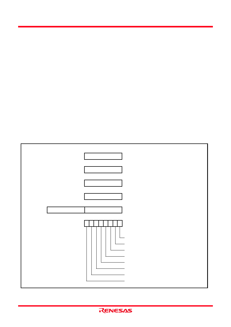
The central processing unit (CPU) has six registers. Figure 5
shows the 740 Family CPU register structure.
[Accumulator (A)]
The accumulator is an 8-bit register. Data operations such as
arithmetic data transfer, etc., are executed mainly through the
accumulator.
[Index Register X (X)]
The index register X is an 8-bit register. In the index addressing
modes, the value of the OPERAND is added to the contents of
register X and specifies the real address.
[Index Register Y (Y)]
The index register Y is an 8-bit register. In partial instruction, the
value of the OPERAND is added to the contents of register Y
and specifies the real address.
[Stack Pointer (S)]
The stack pointer is an 8-bit register used during subroutine calls
and interrupts. This register indicates start address of stored area
(stack) for storing registers during subroutine calls and
interrupts.
The low-order 8 bits of the stack address are determined by the
contents of the stack pointer. The high-order 8 bits of the stack
address are determined by the stack page selection bit. If the
stack page selection bit is “0”, the high-order 8 bits becomes
“0016”. If the stack page selection bit is “1”, the high-order 8 bits
becomes “0116”.
The operations of pushing register contents onto the stack and
popping them from the stack are shown in Figure 6.
Table 6 shows the push and pop instructions of accumulator or
processor status register.
Store registers other than those described in Figure 6 with
program when the user needs them during interrupts or
subroutine calls.
[Program Counter (PC)]
The program counter is a 16-bit counter consisting of two 8-bit
registers PCH and PCL. It is used to indicate the address of the
next instruction to be executed.
Fig. 5 740 Family CPU register structure
Processor status register (PS)
Carry flag
Zero flag
Interrupt disable flag
Decimal mode flag
Break flag
Index X mode flag
Overflow flag
Negative flag
b7
b0
b15
Program counter
Stack pointer
Index register Y
Index register X
Accumulator
A
X
Y
S
PCL
PCH
C
Z
I
D
B
T
V
N
b7
b0
b7
b0
b7
b0
b7
b0
b7
b0
相关PDF资料 |
PDF描述 |
|---|---|
| MC68HC05C9ACB | 8-BIT, MROM, 2.1 MHz, MICROCONTROLLER, PDIP42 |
| MC68HC05C9ACFB | 8-BIT, MROM, 2.1 MHz, MICROCONTROLLER, PQFP44 |
| MC68HC05C9ACFN | 8-BIT, MROM, 2.1 MHz, MICROCONTROLLER, PQCC44 |
| MC68HC908EY16AKFA | 8-BIT, FLASH, 8 MHz, MICROCONTROLLER, PQFP32 |
| MC68HC908EY16AVFA | 8-BIT, FLASH, 8 MHz, MICROCONTROLLER, PQFP32 |
相关代理商/技术参数 |
参数描述 |
|---|---|
| M38D29FFHP#U1 | 制造商:Renesas Electronics Corporation 功能描述: |
| M38D29GFHP#U0 | 制造商:Renesas Electronics Corporation 功能描述: |
| M38D29T2-RLFS-HP | 制造商:Renesas Electronics Corporation 功能描述: |
| M38D58G8FP#U0 | 功能描述:IC 740/38D5 MCU QZ-ROM 80QFP RoHS:是 类别:集成电路 (IC) >> 嵌入式 - 微控制器, 系列:740/38000 标准包装:250 系列:80C 核心处理器:8051 芯体尺寸:8-位 速度:16MHz 连通性:EBI/EMI,I²C,UART/USART 外围设备:POR,PWM,WDT 输入/输出数:40 程序存储器容量:- 程序存储器类型:ROMless EEPROM 大小:- RAM 容量:256 x 8 电压 - 电源 (Vcc/Vdd):4.5 V ~ 5.5 V 数据转换器:A/D 8x10b 振荡器型:内部 工作温度:-40°C ~ 85°C 封装/外壳:68-LCC(J 形引线) 包装:带卷 (TR) |
| M38D58G8HP#U0 | 功能描述:IC 740/38D5 MCU QZ-ROM 80LQFP RoHS:是 类别:集成电路 (IC) >> 嵌入式 - 微控制器, 系列:740/38000 标准包装:250 系列:80C 核心处理器:8051 芯体尺寸:8-位 速度:16MHz 连通性:EBI/EMI,I²C,UART/USART 外围设备:POR,PWM,WDT 输入/输出数:40 程序存储器容量:- 程序存储器类型:ROMless EEPROM 大小:- RAM 容量:256 x 8 电压 - 电源 (Vcc/Vdd):4.5 V ~ 5.5 V 数据转换器:A/D 8x10b 振荡器型:内部 工作温度:-40°C ~ 85°C 封装/外壳:68-LCC(J 形引线) 包装:带卷 (TR) |
发布紧急采购,3分钟左右您将得到回复。