- 您现在的位置:买卖IC网 > PDF目录80580 > M38K27M4L-XXXHP 8-BIT, MROM, 8 MHz, MICROCONTROLLER, PQFP64 PDF资料下载
参数资料
| 型号: | M38K27M4L-XXXHP |
| 元件分类: | 微控制器/微处理器 |
| 英文描述: | 8-BIT, MROM, 8 MHz, MICROCONTROLLER, PQFP64 |
| 封装: | 10 X 10 MM, 0.50 MM PITCH, PLASTIC, LQFP-64 |
| 文件页数: | 4/151页 |
| 文件大小: | 1403K |
| 代理商: | M38K27M4L-XXXHP |
第1页第2页第3页当前第4页第5页第6页第7页第8页第9页第10页第11页第12页第13页第14页第15页第16页第17页第18页第19页第20页第21页第22页第23页第24页第25页第26页第27页第28页第29页第30页第31页第32页第33页第34页第35页第36页第37页第38页第39页第40页第41页第42页第43页第44页第45页第46页第47页第48页第49页第50页第51页第52页第53页第54页第55页第56页第57页第58页第59页第60页第61页第62页第63页第64页第65页第66页第67页第68页第69页第70页第71页第72页第73页第74页第75页第76页第77页第78页第79页第80页第81页第82页第83页第84页第85页第86页第87页第88页第89页第90页第91页第92页第93页第94页第95页第96页第97页第98页第99页第100页第101页第102页第103页第104页第105页第106页第107页第108页第109页第110页第111页第112页第113页第114页第115页第116页第117页第118页第119页第120页第121页第122页第123页第124页第125页第126页第127页第128页第129页第130页第131页第132页第133页第134页第135页第136页第137页第138页第139页第140页第141页第142页第143页第144页第145页第146页第147页第148页第149页第150页第151页
38K2 Group
Rev.3.00
Oct 15, 2006
page 101 of 147
REJ03B0193-0300
Outline Performance (CPU Rewrite Mode)
CPU rewrite mode is usable in the single-chip or Boot mode. The
only User ROM area can be rewritten in CPU rewrite mode.
In CPU rewrite mode, the CPU erases, programs and reads the in-
ternal flash memory as instructed by software commands. This
rewrite control program must be transferred to a memory such as
the internal RAM before it can be executed.
The MCU enters CPU rewrite mode by applying 4.50 V to 5.25 V
to the CNVSS pin and setting “1” to the CPU Rewrite Mode Select
Bit (bit 1 of address 0FFE16). Software commands are accepted
once the mode is entered.
Use software commands to control program and erase operations.
Whether a program or erase operation has terminated normally or
in error can be verified by reading the status register.
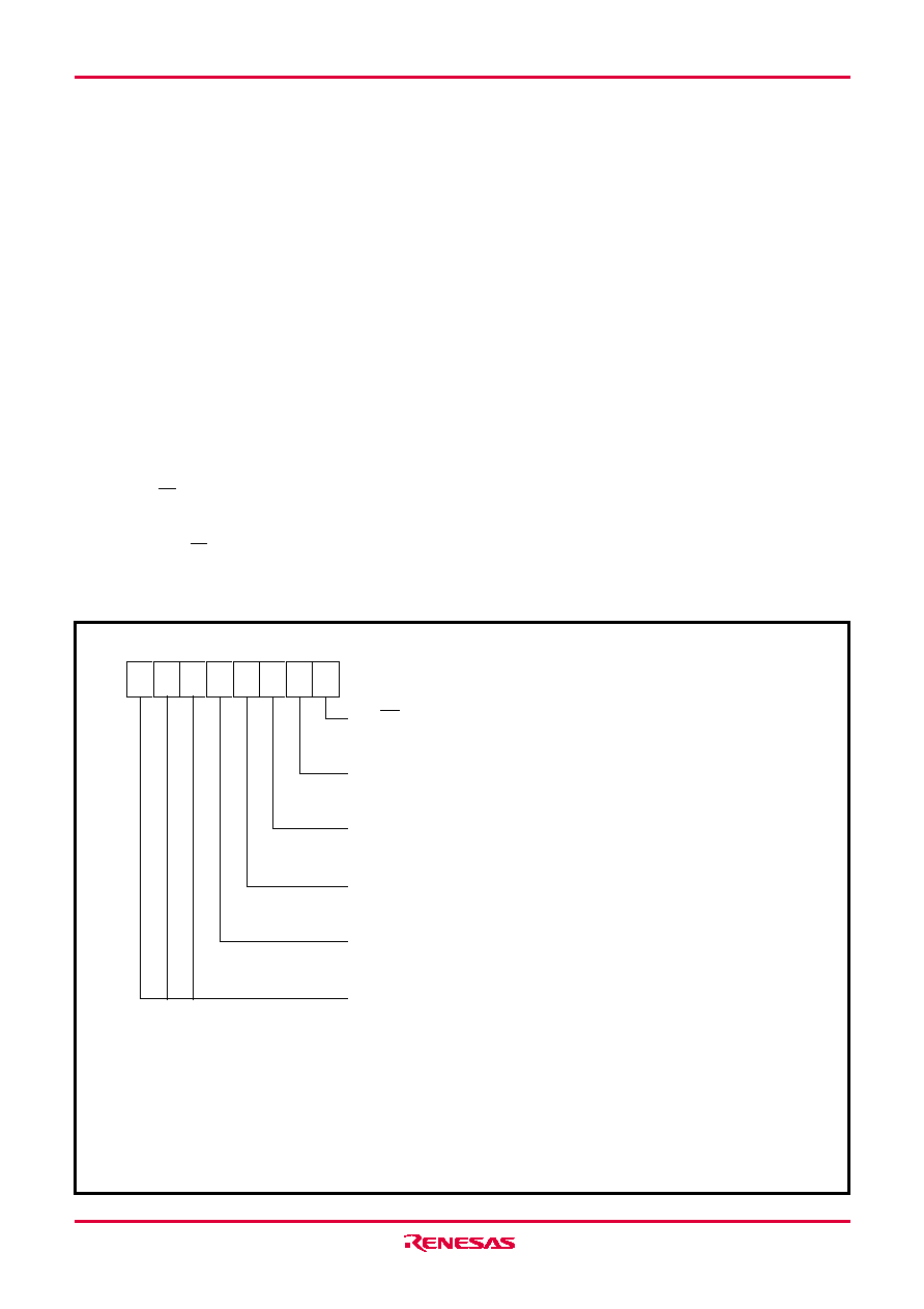
Figure 147 shows the flash memory control register.
Bit 0 is the RY/BY status flag used exclusively to read the operat-
ing status of the flash memory. During programming and erase
operations, it is “0” (busy). Otherwise, it is “1” (ready). This is
equivalent to the RY/BY pin function in parallel I/O mode.
Bit 1 is the CPU Rewrite Mode Select Bit. When this bit is set to
“1”, the MCU enters CPU rewrite mode. Software commands are
accepted once the mode is entered. In CPU rewrite mode, the
Flash memory control register (address 0FFE16)
FMCR (Note 1)
RY/BY status flag
0: Busy (being written or erased)
1: Ready
CPU rewrite mode select bit (Note 2)
0: Normal mode (Software commands invalid)
1: CPU rewrite mode (Software commands acceptable)
CPU rewrite mode entry flag
0: Normal mode (Software commands invalid)
1: CPU rewrite mode
Flash memory reset bit (Note 3)
0: Normal operation
1: Reset
User area / Boot area select bit (Note 4)
0: User ROM area accessed
1: Boot ROM area accessed
Reserved bits (indefinite at read/ “0” at write)
b0
b7
Notes1: The contents of flash memory control register are “XXX00001” just after reset release.
2: For this bit to be set to “1”, the user needs to write “0” and then “1” to it in succession. If it is not
this procedure, this bit will not be set to ”1”. Additionally, it is required to ensure that no interrupt
will be generated during that interval.
Use the control program in the area except the built-in flash memory for write to this bit.
3: This bit is valid when the CPU rewrite mode select bit is “1”. Set this bit 3 to “0” subsequently after
setting bit 3 to “1”.
4: Use the control program in the area except the built-in flash memory for write to this bit.
CPU becomes unable to access the internal flash memory directly.
Therefore, use the control program in a memory other than inter-
nal flash memory for write to bit 1. To set this bit to “1”, it is
necessary to write “0” and then write “1” in succession. The bit can
be set to “0” by only writing “0”.
Bit 2 is the CPU Rewrite Mode Entry Flag. This flag indicates “1” in
CPU rewrite mode, so that reading this flag can check whether
CPU rewrite mode has been entered or not.
Bit 3 is the flash memory reset bit used to reset the control circuit
of internal flash memory. This bit is used when exiting CPU rewrite
mode and when flash memory access has failed. When the CPU
Rewrite Mode Select Bit is “1”, setting “1” for this bit resets the
control circuit. To set this bit to “1”, it is necessary to write “0” and
then write “1” in succession. To release the reset, it is necessary
to set this bit to “0”.
Bit 4 is the User Area/Boot Area Select Bit. When this bit is set to
“1”, Boot ROM area is accessed, and CPU rewrite mode in Boot
ROM area is available. In Boot mode, this bit is set to “1” auto-
matically. Reprogramming of this bit must be in a memory other
than internal flash memory.
Figure 148 shows a flowchart for setting/releasing CPU rewrite
mode.
Fig. 147 Structure of flash memory control register
相关PDF资料 |
PDF描述 |
|---|---|
| M30302MC-XXXFP | 16-BIT, MROM, 16 MHz, MICROCONTROLLER, PQFP100 |
| M37480E8-XXXSP | 8-BIT, OTPROM, 4 MHz, MICROCONTROLLER, PDIP32 |
| M38034M4H-XXXFP | 8-BIT, MROM, 8.4 MHz, MICROCONTROLLER, PQFP64 |
| M30201F6FP | 16-BIT, FLASH, 10 MHz, MICROCONTROLLER, PQFP56 |
| M30620MCP-XXXGP | 16-BIT, MROM, 24 MHz, MICROCONTROLLER, PQFP100 |
相关代理商/技术参数 |
参数描述 |
|---|---|
| M38K29F8LHP | 功能描述:IC 740 MCU FLASH 32K 64LQFP RoHS:否 类别:集成电路 (IC) >> 嵌入式 - 微控制器, 系列:740/38000 产品培训模块:MCU Product Line Introduction XMEGA Introduction AVR XMEGA USB Connectivity 标准包装:90 系列:AVR® XMEGA 核心处理器:AVR 芯体尺寸:8/16-位 速度:32MHz 连通性:I²C,IrDA,SPI,UART/USART 外围设备:欠压检测/复位,DMA,POR,PWM,WDT 输入/输出数:50 程序存储器容量:192KB(96K x 16) 程序存储器类型:闪存 EEPROM 大小:4K x 8 RAM 容量:16K x 8 电压 - 电源 (Vcc/Vdd):1.6 V ~ 3.6 V 数据转换器:A/D 16x12b; D/A 2x12b 振荡器型:内部 工作温度:-40°C ~ 85°C 封装/外壳:64-TQFP 包装:托盘 配用:ATSTK600-RC14-ND - STK600 SOCKET/ADAPTER 64TQFPATSTK600-TQFP64-ND - STK600 SOCKET/ADAPTER 64-TQFPATAVRONEKIT-ND - KIT AVR/AVR32 DEBUGGER/PROGRMMRATAVRISP2-ND - PROGRAMMER AVR IN SYSTEM |
| M38K29F8LHP#U0 | 功能描述:IC 740/38K2 MCU FLASH 64-LQFP RoHS:是 类别:集成电路 (IC) >> 嵌入式 - 微控制器, 系列:740/38000 产品培训模块:CAN Basics Part-1 CAN Basics Part-2 Electromagnetic Noise Reduction Techniques Part 1 M16C Product Overview Part 1 M16C Product Overview Part 2 标准包装:1 系列:M16C™ M32C/80/87 核心处理器:M32C/80 芯体尺寸:16/32-位 速度:32MHz 连通性:EBI/EMI,I²C,IEBus,IrDA,SIO,UART/USART 外围设备:DMA,POR,PWM,WDT 输入/输出数:121 程序存储器容量:384KB(384K x 8) 程序存储器类型:闪存 EEPROM 大小:- RAM 容量:24K x 8 电压 - 电源 (Vcc/Vdd):3 V ~ 5.5 V 数据转换器:A/D 34x10b,D/A 2x8b 振荡器型:内部 工作温度:-20°C ~ 85°C 封装/外壳:144-LQFP 包装:托盘 产品目录页面:749 (CN2011-ZH PDF) 配用:R0K330879S001BE-ND - KIT DEV RSK M32C/87 |
| M38K29F8LHP#UO | 制造商:Renesas Electronics Corporation 功能描述: |
| M38K29T-ADF | 功能描述:DEV TEMPORARY TARGET BOARD FOR M RoHS:否 类别:编程器,开发系统 >> 配件 系列:- 产品培训模块:Lead (SnPb) Finish for COTS Obsolescence Mitigation Program RoHS指令信息:IButton RoHS Compliance Plan 标准包装:1 系列:- 附件类型:USB 至 1-Wire? RJ11 适配器 适用于相关产品:1-Wire? 设备 产品目录页面:1429 (CN2011-ZH PDF) |
| M38K29T-PAC | 制造商:Renesas Electronics Corporation 功能描述:DEV SIMPLE TOOL SYSTEM PKG FOR 38000/38K - Bulk |
发布紧急采购,3分钟左右您将得到回复。