- 您现在的位置:买卖IC网 > PDF目录180212 > M4-128/64-15VC (LATTICE SEMICONDUCTOR CORP) High Performance E 2 CMOS In-System Programmable Logic PDF资料下载
参数资料
| 型号: | M4-128/64-15VC |
| 厂商: | LATTICE SEMICONDUCTOR CORP |
| 元件分类: | PLD |
| 英文描述: | High Performance E 2 CMOS In-System Programmable Logic |
| 中文描述: | EE PLD, 15 ns, PQFP100 |
| 封装: | TQFP-100 |
| 文件页数: | 8/46页 |
| 文件大小: | 754K |
| 代理商: | M4-128/64-15VC |
第1页第2页第3页第4页第5页第6页第7页当前第8页第9页第10页第11页第12页第13页第14页第15页第16页第17页第18页第19页第20页第21页第22页第23页第24页第25页第26页第27页第28页第29页第30页第31页第32页第33页第34页第35页第36页第37页第38页第39页第40页第41页第42页第43页第44页第45页第46页
16
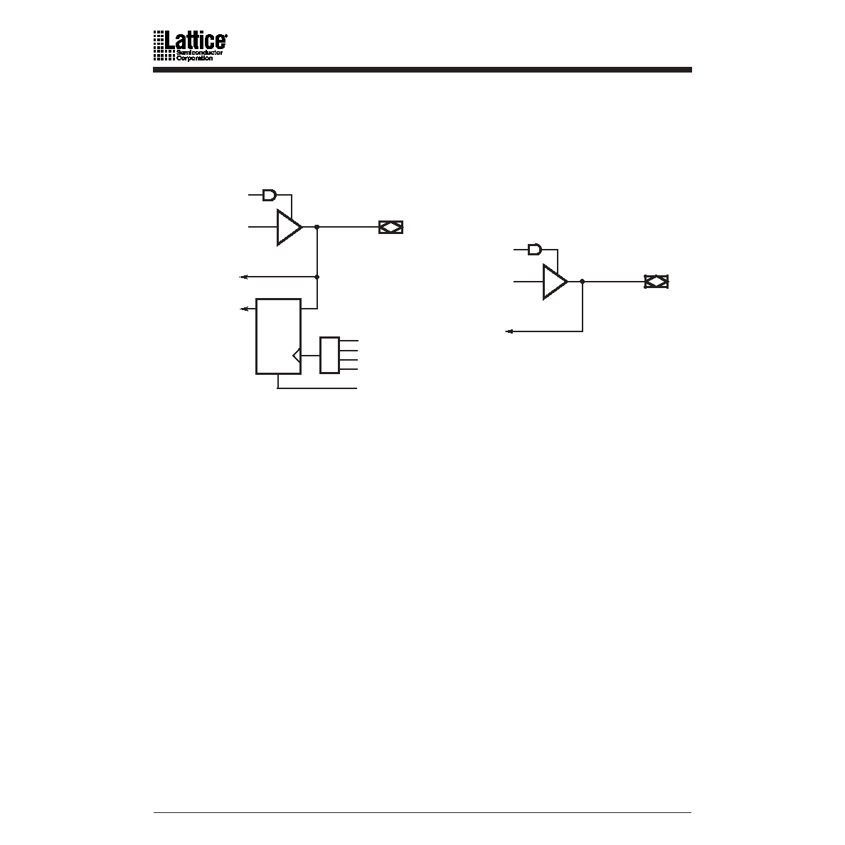
MACH 4 Family
I/O Cell
path, and ip-op (except MACH 4 devices with 1:1 macrocell-I/O cell ratio.) An individual
output enable product term is provided for each I/O cell. The feedback signal drives the input
switch matrix.
The I/O cell (Figure 10) contains a ip-op, which provides the capability for storing the input
in a D-type register or latch. The clock can be any of the PAL block clocks. Both the direct and
registered versions of the input are sent to the input switch matrix. This allows for such functions
as “time-domain-multiplexed” data comparison, where the rst data value is stored, and then the
second data value is put on the I/O pin and compared with the previous stored value.
Note that the ip-op used in the MACH 4 I/O cell is independent of the ip-ops in the
macrocells. It powers up to a logic low.
Zero-Hold-Time Input Register
The MACH 4 devices have a zero-hold-time (ZHT) fuse which controls the time delay associated
with loading data into all I/O cell registers and latches. When programmed, the ZHT fuse
increases the data path setup delays to input storage elements, matching equivalent delays in
the clock path. When the fuse is erased, the setup time to the input storage element is minimized.
This feature facilitates doing worst-case designs for which data is loaded from sources which
have low (or zero) minimum output propagation delays from clock edges.
Input Switch Matrix
matrix. Without the input switch matrix, each input and feedback signal has only one way to
enter the central switch matrix. The input switch matrix provides additional ways for these
signals to enter the central switch matrix.
D/L
Q
Block CLK3
Block CLK2
Block CLK1
Block CLK0
To
Input
Switch
Matrix
Individual
Output Enable
Product Term
From Output
Switch Matrix
17466G-017
17466G-018
Figure 10. I/O Cell for MACH 4 Devices with 2:1
Macrocell-I/O Cell Ratio
Figure 11. I/O Cell for MACH 4 Devices with 1:1
Macrocell-I/O Cell Ratio
To
Input
Switch
Matrix
Individual
Output Enable
Product Term
From Output
Switch Matrix
Power-up reset
相关PDF资料 |
PDF描述 |
|---|---|
| M4-128/64-15YC | High Performance E 2 CMOS In-System Programmable Logic |
| M4-128/64-18VI | High Performance E 2 CMOS In-System Programmable Logic |
| M4-128/64-18YI | High Performance E 2 CMOS In-System Programmable Logic |
| M4-128/64-7VC | High Performance E 2 CMOS In-System Programmable Logic |
| M4-128/64-7YC | High Performance E 2 CMOS In-System Programmable Logic |
相关代理商/技术参数 |
参数描述 |
|---|---|
| M4-128N/64-10JC | 功能描述:CPLD - 复杂可编程逻辑器件 Use ispMACH 4000V or M4A5 RoHS:否 制造商:Lattice 系列: 存储类型:EEPROM 大电池数量:128 最大工作频率:333 MHz 延迟时间:2.7 ns 可编程输入/输出端数量:64 工作电源电压:3.3 V 最大工作温度:+ 90 C 最小工作温度:0 C 封装 / 箱体:TQFP-100 |
| M4-128N/64-10JI | 功能描述:CPLD - 复杂可编程逻辑器件 Use ispMACH 4000V or M4A5 RoHS:否 制造商:Lattice 系列: 存储类型:EEPROM 大电池数量:128 最大工作频率:333 MHz 延迟时间:2.7 ns 可编程输入/输出端数量:64 工作电源电压:3.3 V 最大工作温度:+ 90 C 最小工作温度:0 C 封装 / 箱体:TQFP-100 |
| M4-128N/64-12JC | 功能描述:CPLD - 复杂可编程逻辑器件 Use ispMACH 4000V or M4A5 RoHS:否 制造商:Lattice 系列: 存储类型:EEPROM 大电池数量:128 最大工作频率:333 MHz 延迟时间:2.7 ns 可编程输入/输出端数量:64 工作电源电压:3.3 V 最大工作温度:+ 90 C 最小工作温度:0 C 封装 / 箱体:TQFP-100 |
| M4-128N/64-12JI | 功能描述:CPLD - 复杂可编程逻辑器件 Use ispMACH 4000V or M4A5 RoHS:否 制造商:Lattice 系列: 存储类型:EEPROM 大电池数量:128 最大工作频率:333 MHz 延迟时间:2.7 ns 可编程输入/输出端数量:64 工作电源电压:3.3 V 最大工作温度:+ 90 C 最小工作温度:0 C 封装 / 箱体:TQFP-100 |
| M4-128N/64-14JI | 功能描述:CPLD - 复杂可编程逻辑器件 Use ispMACH 4000V or M4A5 RoHS:否 制造商:Lattice 系列: 存储类型:EEPROM 大电池数量:128 最大工作频率:333 MHz 延迟时间:2.7 ns 可编程输入/输出端数量:64 工作电源电压:3.3 V 最大工作温度:+ 90 C 最小工作温度:0 C 封装 / 箱体:TQFP-100 |
发布紧急采购,3分钟左右您将得到回复。