- 您现在的位置:买卖IC网 > PDF目录45049 > M41ST84YMH6E (STMICROELECTRONICS) 1 TIMER(S), REAL TIME CLOCK, PDSO28 PDF资料下载
参数资料
| 型号: | M41ST84YMH6E |
| 厂商: | STMICROELECTRONICS |
| 元件分类: | 时钟/数据恢复及定时提取 |
| 英文描述: | 1 TIMER(S), REAL TIME CLOCK, PDSO28 |
| 封装: | 0.330 INCH, LEAD FREE, PLASTIC, SOH-28 |
| 文件页数: | 3/31页 |
| 文件大小: | 507K |
| 代理商: | M41ST84YMH6E |
第1页第2页当前第3页第4页第5页第6页第7页第8页第9页第10页第11页第12页第13页第14页第15页第16页第17页第18页第19页第20页第21页第22页第23页第24页第25页第26页第27页第28页第29页第30页第31页
11/31
M41ST84Y, M41ST84W
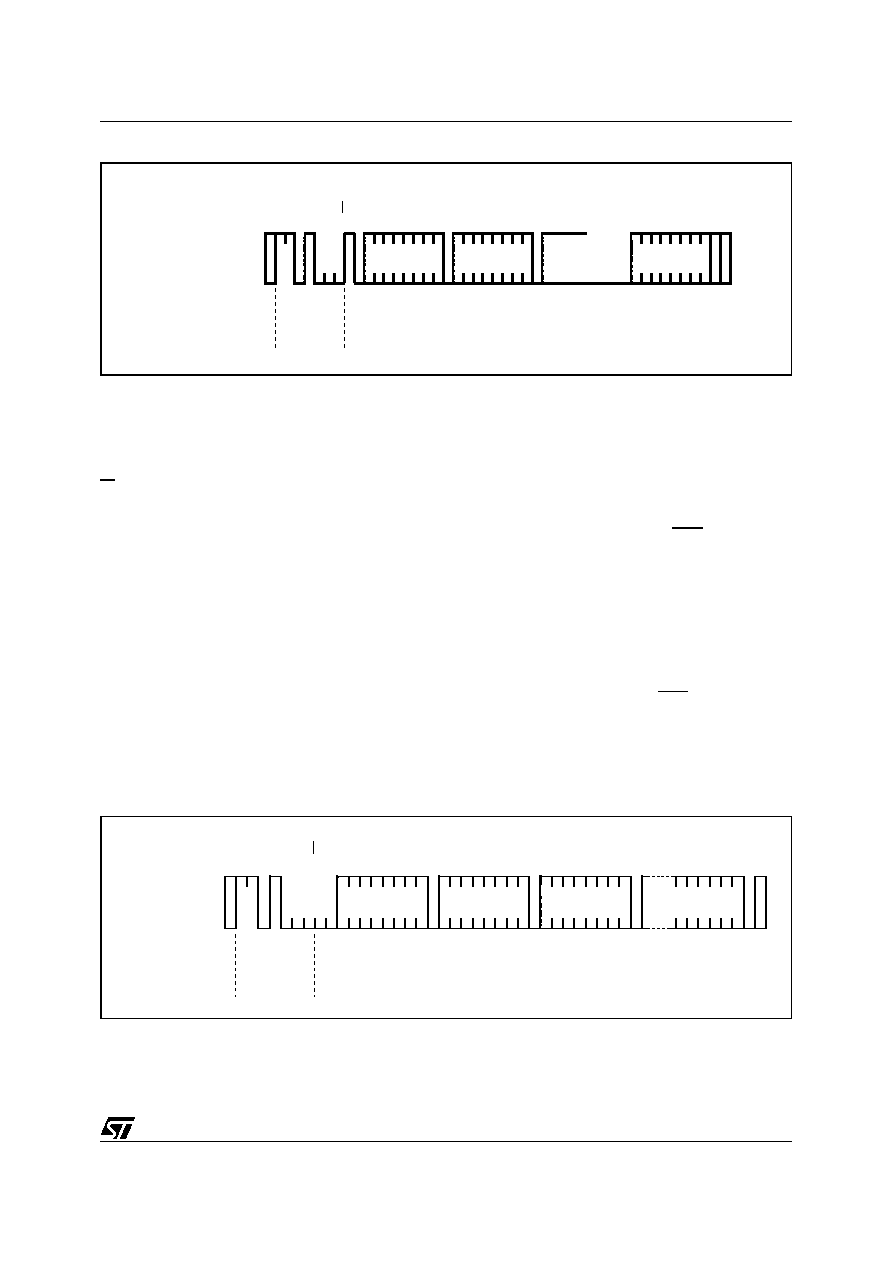
Figure 13. Alternate READ Mode Sequence
WRITE Mode
In this mode the master transmitter transmits to
the M41ST84Y/W slave receiver. Bus protocol is
shown in Figure 14., page 11. Following the
START condition and slave address, a logic '0' (R/
W=0) is placed on the bus and indicates to the ad-
dressed device that word address An will follow
and is to be written to the on-chip address pointer.
The data word to be written to the memory is
strobed in next and the internal address pointer is
incremented to the next memory location within
the RAM on the reception of an acknowledge
clock. The M41ST84Y/W slave receiver will send
an acknowledge clock to the master transmitter af-
ter it has received the slave address (see Figure
11., page 10) and again after it has received the
word address and each data byte.
Data Retention Mode
With valid VCC applied, the M41ST84Y/W can be
accessed as described above with READ or
WRITE cycles. Should the supply voltage decay,
the M41ST84Y/W will automatically deselect,
write protecting itself when VCC falls between
VPFD(max) and VPFD(min). This is accomplished
by internally inhibiting access to the clock regis-
ters. At this time, the Reset pin (RST) is driven ac-
tive and will remain active until VCC returns to
nominal levels. When VCC falls below the Battery
Back-up Switchover Voltage (VSO), power input is
switched from the VCC pin to the SNAPHAT
(or
external) battery, and the clock registers and
SRAM are maintained from the attached battery
supply.
All outputs become high impedance. On power up,
when VCC returns to a nominal value, write protec-
tion continues for tREC. The RST signal also re-
mains
active
during
this
time
(see
For a further more detailed review of lifetime calcu-
lations, please see Application Note AN1012.
Figure 14. WRITE Mode Sequence
AI00895
BUS ACTIVITY:
ACK
S
ACK
NO
ACK
STOP
START
P
SDA LINE
BUS ACTIVITY:
MASTER
R/W
DATA n
DATA n+1
DATA n+X
SLAVE
ADDRESS
AI00591
BUS ACTIVITY:
ACK
S
ACK
STOP
START
P
SDA LINE
BUS ACTIVITY:
MASTER
R/W
DATA n
DATA n+1
DATA n+X
WORD
ADDRESS (An)
SLAVE
ADDRESS
相关PDF资料 |
PDF描述 |
|---|---|
| M41ST85Y-70MH6 | 1 TIMER(S), REAL TIME CLOCK, PDSO28 |
| M41ST85Y-85MH6TR | 1 TIMER(S), REAL TIME CLOCK, PDSO28 |
| M41ST85Y-85MH6 | 1 TIMER(S), REAL TIME CLOCK, PDSO28 |
| M41ST87YWX6 | 1 TIMER(S), REAL TIME CLOCK, PDSO28 |
| M41T00M6F | REAL TIME CLOCK, PDSO8 |
相关代理商/技术参数 |
参数描述 |
|---|---|
| M41ST84YMQ | 制造商:STMICROELECTRONICS 制造商全称:STMicroelectronics 功能描述:5.0 or 3.0V, 512 bit 64 x 8 SERIAL RTC with SUPERVISORY FUNCTIONS |
| M41ST84YMQ1 | 制造商:STMICROELECTRONICS 制造商全称:STMicroelectronics 功能描述:5.0 or 3.0V, 512 bit 64 x 8 SERIAL RTC with SUPERVISORY FUNCTIONS |
| M41ST84YMQ1TR | 制造商:STMICROELECTRONICS 制造商全称:STMicroelectronics 功能描述:5.0 or 3.0V, 512 bit 64 x 8 SERIAL RTC with SUPERVISORY FUNCTIONS |
| M41ST84YMQ6 | 功能描述:实时时钟 Serial 512 (64x8) RoHS:否 制造商:Microchip Technology 功能:Clock, Calendar. Alarm RTC 总线接口:I2C 日期格式:DW:DM:M:Y 时间格式:HH:MM:SS RTC 存储容量:64 B 电源电压-最大:5.5 V 电源电压-最小:1.8 V 最大工作温度:+ 85 C 最小工作温度: 安装风格:Through Hole 封装 / 箱体:PDIP-8 封装:Tube |
| M41ST84YMQ6E | 功能描述:IC RTC 5.0V 512BIT NVRAM 16SOIC RoHS:否 类别:集成电路 (IC) >> 时钟/计时 - 实时时钟 系列:- 产品培训模块:Obsolescence Mitigation Program 标准包装:1 系列:- 类型:时钟/日历 特点:警报器,闰年,SRAM 存储容量:- 时间格式:HH:MM:SS(12/24 小时) 数据格式:YY-MM-DD-dd 接口:SPI 电源电压:2 V ~ 5.5 V 电压 - 电源,电池:- 工作温度:-40°C ~ 85°C 安装类型:表面贴装 封装/外壳:8-WDFN 裸露焊盘 供应商设备封装:8-TDFN EP 包装:管件 |
发布紧急采购,3分钟左右您将得到回复。