- 您现在的位置:买卖IC网 > PDF目录69016 > M41ST87WMX6 (STMICROELECTRONICS) 1 TIMER(S), REAL TIME CLOCK, PDSO28 PDF资料下载
参数资料
| 型号: | M41ST87WMX6 |
| 厂商: | STMICROELECTRONICS |
| 元件分类: | 时钟/数据恢复及定时提取 |
| 英文描述: | 1 TIMER(S), REAL TIME CLOCK, PDSO28 |
| 封装: | 0.300 INCH, ROHS COMPLIANT, PLASTIC, SOX-28 |
| 文件页数: | 7/52页 |
| 文件大小: | 689K |
| 代理商: | M41ST87WMX6 |
第1页第2页第3页第4页第5页第6页当前第7页第8页第9页第10页第11页第12页第13页第14页第15页第16页第17页第18页第19页第20页第21页第22页第23页第24页第25页第26页第27页第28页第29页第30页第31页第32页第33页第34页第35页第36页第37页第38页第39页第40页第41页第42页第43页第44页第45页第46页第47页第48页第49页第50页第51页第52页
M41ST87Y, M41ST87W
Operating modes
Doc ID 9497 Rev 8
Table 2.
AC characteristics
2.2
READ mode
In this mode the master reads the M41ST87Y/W slave after setting the slave address (see
Figure 9 on page 16). Following the WRITE mode control bit (R/W=0) and the acknowledge
bit, the word address 'An' is written to the on-chip address pointer. Next the START
condition and slave address are repeated followed by the READ mode control bit (R/W=1).
At this point the master transmitter becomes the master receiver.
The data byte which was addressed will be transmitted and the master receiver will send an
acknowledge bit to the slave transmitter. The address pointer is only incremented on
reception of an acknowledge clock. The M41ST87Y/W slave transmitter will now place the
data byte at address An+1 on the bus, the master receiver reads and acknowledges the new
byte and the address pointer is incremented to An+2.
This cycle of reading consecutive addresses will continue until the master receiver sends a
STOP condition to the slave transmitter (see Figure 10 on page 16).
The system-to-user transfer of clock data will be halted whenever the address being read is
a clock address (00h to 07h). The update will resume either due to a stop condition or when
the pointer increments to a non-clock or RAM address.
Note:
This is true both in READ mode and WRITE mode.
An alternate READ mode may also be implemented whereby the master reads the
M41ST87Y/W slave without first writing to the (volatile) address pointer. The first address
that is read is the last one stored in the pointer (see Figure 11 on page 16).
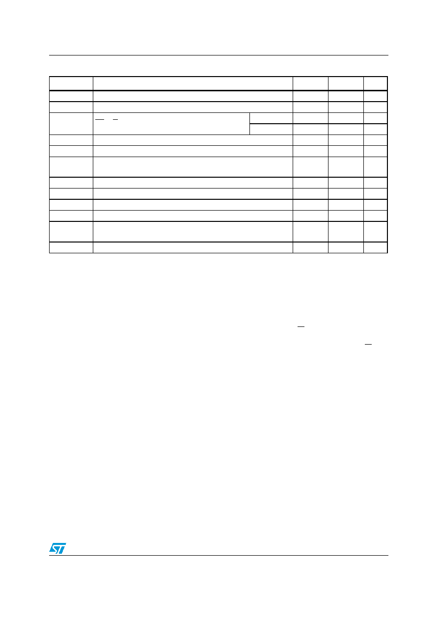
Symbol
Parameter(1)
1.
Valid for ambient operating temperature: TA = –40 to 85 °C; VCC = 4.5 to 5.5 V or 2.7 to 3.6 V (except where noted).
Min
Max
Unit
fSCL
SCL clock frequency
0
400
kHz
tBUF
Time the bus must be free before a new transmission can start
1.3
s
tEXPD
(2)
2.
Available in SOX28 (MX) package only.
EX to ECON propagation delay
M41ST87Y
10
ns
M41ST87W
15
ns
tF
SDA and SCL fall time
300
ns
tHD:DAT
(3)
3.
Transmitter must internally provide a hold time to bridge the undefined region (300 ns max) of the falling edge of SCL.
Data hold time
0
s
tHD:STA
START condition hold time
(after this period the first clock pulse is generated)
600
ns
tHIGH
Clock high period
600
ns
tLOW
Clock low period
1.3
s
tR
SDA and SCL rise time
300
ns
tSU:DAT
Data setup time
100
ns
tSU:STA
START condition setup time
(only relevant for a repeated start condition)
600
ns
tSU:STO
STOP condition setup time
600
ns
相关PDF资料 |
PDF描述 |
|---|---|
| M41ST87YMX6 | 1 TIMER(S), REAL TIME CLOCK, PDSO28 |
| M41ST87YMX6TR | 1 TIMER(S), REAL TIME CLOCK, PDSO28 |
| M41ST87WMX6TR | 1 TIMER(S), REAL TIME CLOCK, PDSO28 |
| M41ST95WMX6 | 1 TIMER(S), REAL TIME CLOCK, PDSO28 |
| M41ST95YMH6E | 1 TIMER(S), REAL TIME CLOCK, PDSO28 |
相关代理商/技术参数 |
参数描述 |
|---|---|
| M41ST87WMX6F | 制造商:STMICROELECTRONICS 制造商全称:STMicroelectronics 功能描述:5.0 V and 3.3/3.0 V secure serial RTC and NVRAM supervisor with tamper detection and 128 bytes of clearable NVRAM |
| M41ST87WMX6TR | 功能描述:实时时钟 Serial 1280 (160x8) RoHS:否 制造商:Microchip Technology 功能:Clock, Calendar. Alarm RTC 总线接口:I2C 日期格式:DW:DM:M:Y 时间格式:HH:MM:SS RTC 存储容量:64 B 电源电压-最大:5.5 V 电源电压-最小:1.8 V 最大工作温度:+ 85 C 最小工作温度: 安装风格:Through Hole 封装 / 箱体:PDIP-8 封装:Tube |
| M41ST87WSS6 | 制造商:STMICROELECTRONICS 制造商全称:STMicroelectronics 功能描述:5.0 V and 3.3/3.0 V secure serial RTC and NVRAM supervisor with tamper detection and 128 bytes of clearable NVRAM |
| M41ST87WSS6F | 功能描述:实时时钟 128 NVRAM Serial RTC 3.0 to 3.6 Vcc RoHS:否 制造商:Microchip Technology 功能:Clock, Calendar. Alarm RTC 总线接口:I2C 日期格式:DW:DM:M:Y 时间格式:HH:MM:SS RTC 存储容量:64 B 电源电压-最大:5.5 V 电源电压-最小:1.8 V 最大工作温度:+ 85 C 最小工作温度: 安装风格:Through Hole 封装 / 箱体:PDIP-8 封装:Tube |
| M41ST87Y | 制造商:STMICROELECTRONICS 制造商全称:STMicroelectronics 功能描述:5.0, 3.3, or 3.0V, 1280 bit (160 x8) Secure Serial RTC and NVRAM Supervisor with Tamper Detection |
发布紧急采购,3分钟左右您将得到回复。