- 您现在的位置:买卖IC网 > PDF目录383300 > M470L3224FT0-CB3 (SAMSUNG SEMICONDUCTOR CO. LTD.) DDR SDRAM SODIMM PDF资料下载
参数资料
| 型号: | M470L3224FT0-CB3 |
| 厂商: | SAMSUNG SEMICONDUCTOR CO. LTD. |
| 英文描述: | DDR SDRAM SODIMM |
| 中文描述: | 的DDR SDRAM SODIMM |
| 文件页数: | 17/20页 |
| 文件大小: | 264K |
| 代理商: | M470L3224FT0-CB3 |
DDR SDRAM
128MB, 256MB SODIMM Pb-Free
Revision 1.2 Oct. 2004
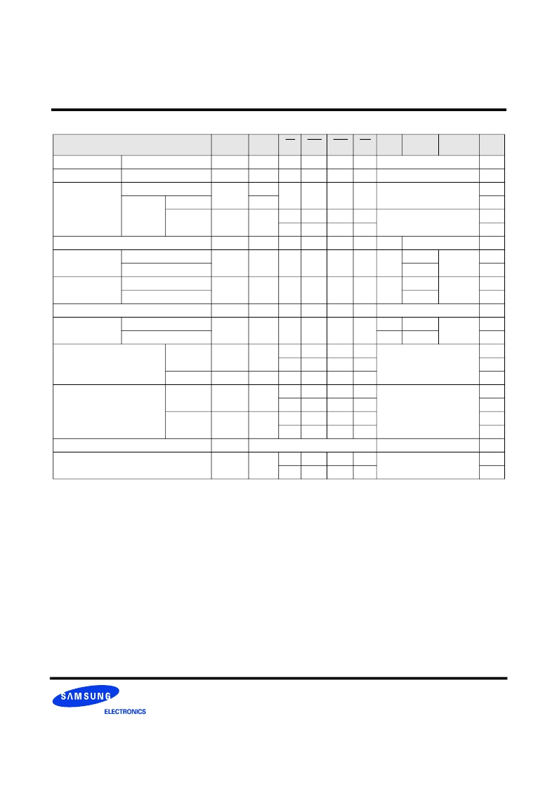
Command Truth Table
(V=Valid, X=Don
′
t Care, H=Logic High, L=Logic Low)
COMMAND
CKEn-1
CKEn
CS
RAS
CAS
WE
BA
0,1
A
10
/AP
A
0
~ A
9,
A
11,
A
12
Note
Register
Extended MRS
H
X
L
L
L
L
OP CODE
1, 2
Register
Mode Register Set
H
X
L
L
L
L
OP CODE
1, 2
Refresh
Auto Refresh
H
H
L
L
L
H
X
3
Self
Refresh
Entry
L
3
Exit
L
H
L
H
H
H
X
3
H
X
X
X
3
Bank Active & Row Addr.
H
X
L
L
H
H
V
Row Address
Read &
Column Address
Auto Precharge Disable
H
X
L
H
L
H
V
L
Column
Address
4
Auto Precharge Enable
H
4
Write &
Column Address
Auto Precharge Disable
H
X
L
H
L
L
V
L
Column
Address
4
Auto Precharge Enable
H
4, 6
Burst Stop
H
X
L
H
H
L
X
7
Precharge
Bank Selection
H
X
L
L
H
L
V
L
X
All Banks
X
H
5
Active Power Down
Entry
H
L
H
X
X
X
X
L
V
V
V
Exit
L
H
X
X
X
X
Precharge Power Down Mode
Entry
H
L
H
X
X
X
X
L
H
H
H
Exit
L
H
H
X
X
X
L
V
V
V
DM
H
X
X
8
No operation (NOP) : Not defined
H
X
H
X
X
X
X
9
L
H
H
H
9
Note : 1. OP Code : Operand Code. A
0
~ A
12
& BA
0
~ BA
1
: Program keys. (@EMRS/MRS)
2. EMRS/ MRS can be issued only at all banks precharge state.
A new command can be issued 2 clock cycles after EMRS or MRS.
3. Auto refresh functions are same as the CBR refresh of DRAM.
The automatical precharge without row precharge command is meant by "Auto".
Auto/self refresh can be issued only at all banks precharge state.
4. BA
0
~ BA
1
: Bank select addresses.
If both BA
0
and BA
1
are "Low" at read, write, row active and precharge, bank A is selected.
If BA
0
is "High" and BA
1
is "Low" at read, write, row active and precharge, bank B is selected.
If BA
0
is "Low" and BA
1
is "High" at read, write, row active and precharge, bank C is selected.
If both BA
0
and BA
1
are "High" at read, write, row active and precharge, bank D is selected.
5. If A
10
/AP is "High" at row precharge, BA
0
and BA
1
are ignored and all banks are selected.
6. During burst write with auto precharge, new read/write command can not be issued.
Another bank read/write command can be issued after the end of burst.
New row active of the associated bank can be issued at t
RP
after the end of burst.
7. Burst stop command is valid at every burst length.
8. DM sampled at the rising and falling edges of the DQS and Data-in are masked at the both edges (Write DM latency is 0).
9. This combination is not defined for any function, which means "No Operation(NOP)" in DDR SDRAM.
相关PDF资料 |
PDF描述 |
|---|---|
| M470L3224BT0 | 256MB DDR SDRAM MODULE |
| M470L3224BTO | 256MB DDR SDRAM MODULE |
| M470L1624FU0-CA2 | DDR SDRAM SODIMM |
| M470L3224FU0-CA2 | Ring Core Bead Ferrite; Impedance:340ohm; Cable Diameter Max:0.203"; Width (Latch Included):1.23"; External Height:1.155"; External Width:1.125"; Length:1.25" |
| M485L1624FU0-CA2 | Ring Core Bead Ferrite; Impedance:200ohm; Cable Diameter Max:0.35"; Latch Height:0.2"; Width (Latch Included):0.885"; External Height:0.79"; External Width:0.77"; Length:1.45" |
相关代理商/技术参数 |
参数描述 |
|---|---|
| M470L3224FU0 | 制造商:SAMSUNG 制造商全称:Samsung semiconductor 功能描述:DDR SDRAM SODIMM |
| M470L3224FU0-CA2 | 制造商:SAMSUNG 制造商全称:Samsung semiconductor 功能描述:DDR SDRAM SODIMM |
| M470L3224FU0-CB0 | 制造商:SAMSUNG 制造商全称:Samsung semiconductor 功能描述:DDR SDRAM SODIMM |
| M470L3224FU0-CB3 | 制造商:SAMSUNG 制造商全称:Samsung semiconductor 功能描述:DDR SDRAM SODIMM |
| M470L3224HU0 | 制造商:SAMSUNG 制造商全称:Samsung semiconductor 功能描述:DDR SDRAM Product Guide |
发布紧急采购,3分钟左右您将得到回复。