- 您现在的位置:买卖IC网 > PDF目录383300 > M470L6423EN0-CLB3 (SAMSUNG SEMICONDUCTOR CO. LTD.) 512MB Unbuffered SODIMM(based on sTSOP) PDF资料下载
参数资料
| 型号: | M470L6423EN0-CLB3 |
| 厂商: | SAMSUNG SEMICONDUCTOR CO. LTD. |
| 英文描述: | 512MB Unbuffered SODIMM(based on sTSOP) |
| 中文描述: | 512MB的无缓冲的SODIMM(基于sTSOP) |
| 文件页数: | 6/13页 |
| 文件大小: | 145K |
| 代理商: | M470L6423EN0-CLB3 |
DDR SDRAM
512MB Unbuffered SODIMM(based on sTSOP)
Rev. 1.3 March. 2004
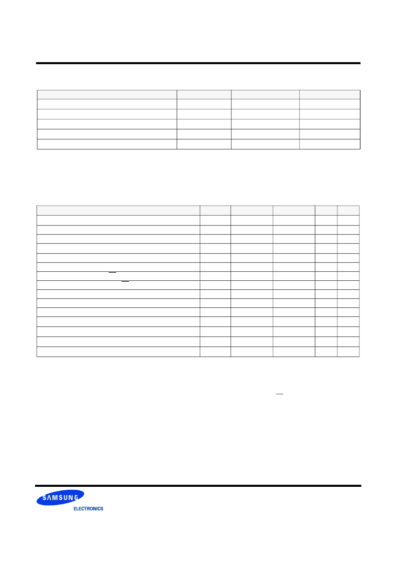
Absolute Maximum Ratings
Parameter
Symbol
V
IN
, V
OUT
V
DD
, V
DDQ
T
STG
P
D
I
OS
Value
-0.5 ~ 3.6
Unit
V
Voltage on any pin relative to V
SS
Voltage on V
DD
& V
DDQ
supply relative to V
SS
Storage temperature
-1.0 ~ 3.6
V
-55 ~ +150
°
C
Power dissipation
1.5 * # of component
W
Short circuit current
50
mA
Note :
Permanent device damage may occur if ABSOLUTE MAXIMUM RATINGS are exceeded.
Functional operation should be restricted to recommend operation condition.
Exposure to higher than recommended voltage for extended periods of time could affect device reliability.
DC Operating Conditions
Recommended operating conditions(Voltage referenced to V
SS
=0V, T
A
=0 to 70
°
C)
Parameter
Symbol
V
DD
Min
2.3
Max
Unit
Note
Supply voltage(for device with a nominal V
DD
of 2.5V)
2.7
I/O Supply voltage
I/O Reference voltage
I/O Termination voltage(system)
V
DDQ
V
REF
V
TT
V
IH
(DC)
V
IL
(DC)
V
IN
(DC)
V
ID
(DC)
VI(Ratio)
I
I
I
OZ
2.3
2.7
V
V
0.49*VDDQ
V
REF
-0.04
0.51*VDDQ
V
REF
+0.04
1
V
2
Input logic high voltage
Input logic low voltage
Input Voltage Level, CK and CK inputs
Input Differential Voltage, CK and CK inputs
V-I Matching: Pullup to Pulldown Current Ratio
Input leakage current
Output leakage current
Output High Current(Normal strengh driver) ;V
OUT
= V
TT
+ 0.84V
Output High Current(Normal strengh driver) ;V
OUT
= V
TT
- 0.84V
Output High Current(Half strengh driver) ;V
OUT
= V
TT
+ 0.45V
Output High Current(Half strengh driver) ;V
OUT
= V
TT
- 0.45V
V
REF
+0.15
-0.3
-0.3
0.36
0.71
-2
-5
V
DDQ
+0.3
V
REF
-0.15
V
DDQ
+0.3
V
DDQ
+0.6
1.4
2
5
V
V
V
V
-
uA
uA
3
4
I
OH
-16.8
mA
I
OL
16.8
mA
I
OH
-9
mA
I
OL
9
mA
1.VREF is expected to be equal to 0.5*VDDQ of the transmitting device, and to track variations in the dc level of same.
Peak-to peak noise on VREF may not exceed +/-2% of the dc value.
2. V
TT
is not applied directly to the device. V
TT
is a system supply for signal termination resistors, is expected to be set equal to
V
REF
, and must track variations in the DC level of V
REF
3. V
ID
is the magnitude of the difference between the input level on CK and the input level on CK.
4. The ratio of the pullup current to the pulldown current is specified for the same temperature and voltage, over the entire
temperature and voltage range, for device drain to source voltages from 0.25V to 1.0V. For a given output, it represents the
maximum difference between pullup and pulldown drivers due to process variation. The full variation in the ratio of the
maximum to minimum pullup and pulldown current will not exceed 1/7 for device drain to source voltages from 0.1 to 1.0.
Note :
相关PDF资料 |
PDF描述 |
|---|---|
| M470L6524CU0 | DDR SDRAM Unbuffered Module 18 4 pin Unbuffered Module based on 512Mb C-die |
| M470L6524CU0-LB3 | DDR SDRAM Unbuffered Module 18 4 pin Unbuffered Module based on 512Mb C-die |
| M470L6524CU0-LCC | DDR SDRAM Unbuffered Module 18 4 pin Unbuffered Module based on 512Mb C-die |
| M470L3324CU0-CA2 | DDR SDRAM Unbuffered Module 18 4 pin Unbuffered Module based on 512Mb C-die |
| M470L6524CU0-CA2 | DDR SDRAM Unbuffered Module 18 4 pin Unbuffered Module based on 512Mb C-die |
相关代理商/技术参数 |
参数描述 |
|---|---|
| M470L6524BT0-CA2 | 制造商:SAMSUNG 制造商全称:Samsung semiconductor 功能描述:DDR SDRAM Unbuffered Module 18 4 pin Unbuffered Module based on 512Mb B-die |
| M470L6524BT0-CB0 | 制造商:SAMSUNG 制造商全称:Samsung semiconductor 功能描述:DDR SDRAM Unbuffered Module 18 4 pin Unbuffered Module based on 512Mb B-die |
| M470L6524BT0-CB3 | 制造商:SAMSUNG 制造商全称:Samsung semiconductor 功能描述:DDR SDRAM Unbuffered Module 18 4 pin Unbuffered Module based on 512Mb B-die |
| M470L6524BT0-CCC | 制造商:SAMSUNG 制造商全称:Samsung semiconductor 功能描述:DDR SDRAM Unbuffered Module 18 4 pin Unbuffered Module based on 512Mb B-die |
| M470L6524BT0-CLA2 | 制造商:SAMSUNG 制造商全称:Samsung semiconductor 功能描述:DDR SDRAM Unbuffered Module 18 4 pin Unbuffered Module based on 512Mb B-die |
发布紧急采购,3分钟左右您将得到回复。