- 您现在的位置:买卖IC网 > PDF目录132964 > M48T08Y-10MH1F (STMICROELECTRONICS) 0 TIMER(S), REAL TIME CLOCK, PDSO28 PDF资料下载
参数资料
| 型号: | M48T08Y-10MH1F |
| 厂商: | STMICROELECTRONICS |
| 元件分类: | 时钟/数据恢复及定时提取 |
| 英文描述: | 0 TIMER(S), REAL TIME CLOCK, PDSO28 |
| 封装: | 0.330 INCH, ROHS COMPLIANT, PLASTIC, SOH-28 |
| 文件页数: | 4/31页 |
| 文件大小: | 256K |
| 代理商: | M48T08Y-10MH1F |
第1页第2页第3页当前第4页第5页第6页第7页第8页第9页第10页第11页第12页第13页第14页第15页第16页第17页第18页第19页第20页第21页第22页第23页第24页第25页第26页第27页第28页第29页第30页第31页
Operation modes
M48T08, M48T08Y, M48T18
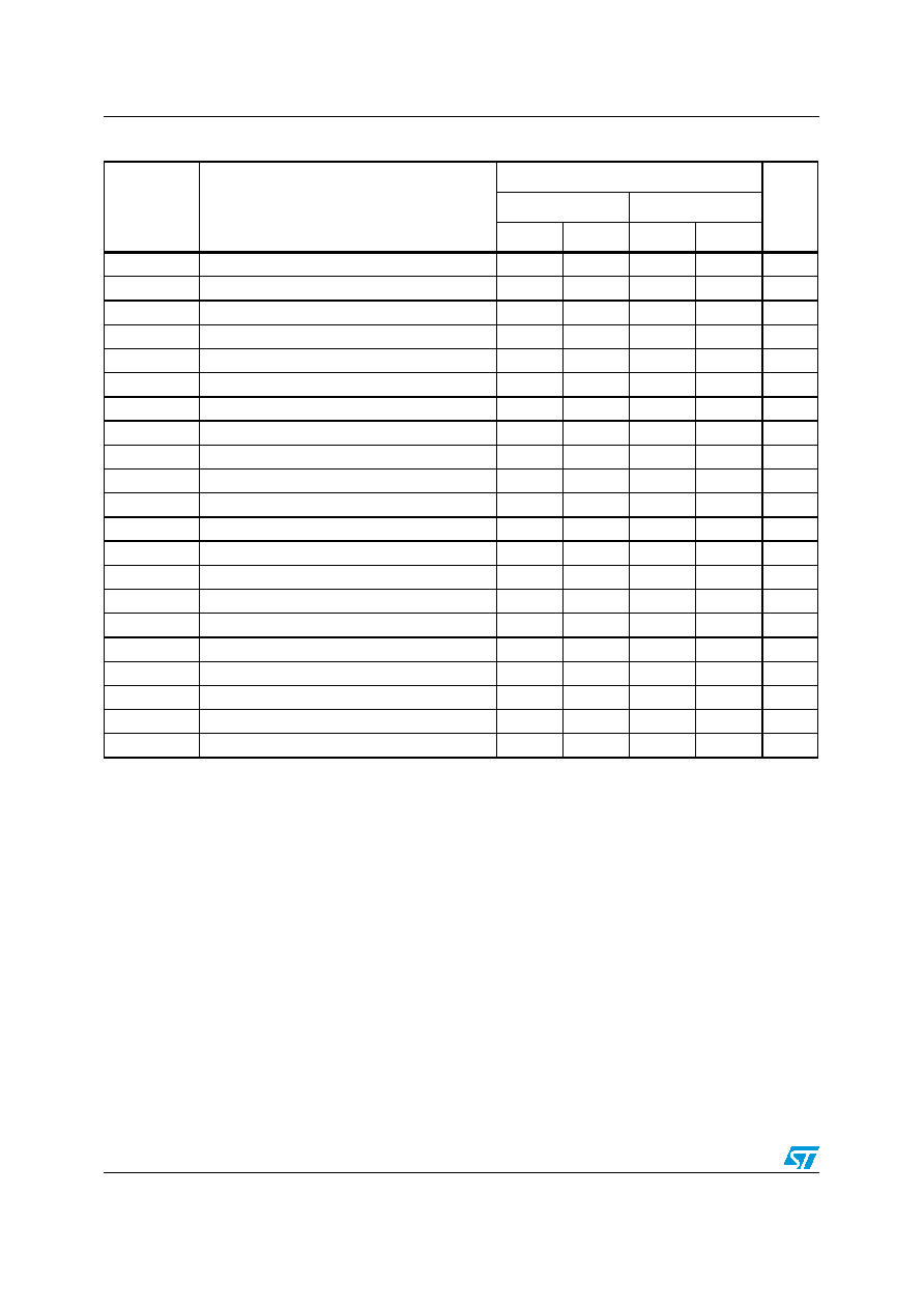
Table 4.
Write mode AC characteristics
2.3
Data retention mode
With valid VCC applied, the M48T08/18/08Y operates as a conventional BYTEWIDE static
RAM. Should the supply voltage decay, the RAM will automatically power-fail deselect, write
protecting itself when VCC falls within the VPFD (max), VPFD (min) window. All outputs
become high impedance, and all inputs are treated as “Don't care.”
Note:
A power failure during a WRITE cycle may corrupt data at the currently addressed location,
but does not jeopardize the rest of the RAM's content. At voltages below VPFD (min), the
user can be assured the memory will be in a write protected state, provided the VCC fall time
is not less than tF. The M48T08/18/08Y may respond to transient noise spikes on VCC that
reach into the deselect window during the time the device is sampling VCC. Therefore,
decoupling of the power supply lines is recommended.
Symbol
Parameter(1)
1.
Valid for ambient operating temperature: TA = 0 to 70°C; VCC = 4.75 to 5.5 V or 4.5 to 5.5 V (except where noted).
M48T08/M48T18/T08Y
Unit
–100/–10 (T08Y)
–150/–15 (T08Y)
MinMax
tAVAV
WRITE cycle time
100
150
ns
tAVWL
Address valid to WRITE enable low
0
ns
tAVE1L
Address valid to chip enable 1 low
0
ns
tAVE2H
Address valid to chip enable 2 high
0
ns
tWLWH
WRITE enable pulse width
80
100
ns
tE1LE1H
Chip enable 1 low to chip enable 1 high
80
130
ns
tE2HE2L
Chip enable 2 high to chip enable 2 low
80
130
ns
tWHAX
WRITE enable high to address transition
10
ns
tE1HAX
Chip enable 1 high to address transition
10
ns
tE2LAX
Chip enable 2 low to address transition
10
ns
tDVWH
Input valid to WRITE enable high
50
70
ns
tDVE1H
Input valid to chip enable 1 high
50
70
ns
tDVE2L
Input valid to chip enable 2 low
50
70
ns
tWHDX
WRITE enable high to input transition
5
ns
tE1HDX
Chip enable 1 high to input transition
5
ns
tE2LDX
Chip enable 2 low to input transition
5
ns
tWLQZ
WRITE enable low to output Hi-Z
50
70
ns
tAVWH
Address valid to WRITE enable high
80
130
ns
tAVE1H
Address valid to chip enable 1 high
80
130
ns
tAVE2L
Address valid to chip enable 2 low
80
130
ns
tWHQX
WRITE enable high to output transition
10
ns
相关PDF资料 |
PDF描述 |
|---|---|
| MK2703SILFTR | 27 MHz, OTHER CLOCK GENERATOR, PDSO8 |
| MC9S08RE16CFG | 8-BIT, FLASH, 8 MHz, MICROCONTROLLER, PQFP44 |
| MC9S08RE16CFJ | 8-BIT, FLASH, 8 MHz, MICROCONTROLLER, PQFP32 |
| MC68HC05L16FU | 8-BIT, MROM, 2.1 MHz, MICROCONTROLLER, PQFP80 |
| MC68HC05P18AMDW | 8-BIT, MROM, 2.1 MHz, MICROCONTROLLER, PDSO28 |
相关代理商/技术参数 |
参数描述 |
|---|---|
| M48T08Y-10MH1F(LOOSE)-XYZ | 制造商:STMicroelectronics 功能描述: |
| M48T08Y-10MH1TR | 制造商:STMICROELECTRONICS 制造商全称:STMicroelectronics 功能描述:64 Kbit 8Kb x 8 TIMEKEEPER SRAM |
| M48T08Y-10PC1 | 制造商:STMICROELECTRONICS 制造商全称:STMicroelectronics 功能描述:64 Kbit 8Kb x 8 TIMEKEEPER SRAM |
| M48T08Y-10PC1E | 制造商:STMICROELECTRONICS 制造商全称:STMicroelectronics 功能描述:64 Kbit 8Kb x 8 TIMEKEEPER SRAM |
| M48T08Y-10PC1F | 制造商:STMICROELECTRONICS 制造商全称:STMicroelectronics 功能描述:64 Kbit 8Kb x 8 TIMEKEEPER SRAM |
发布紧急采购,3分钟左右您将得到回复。