- 您现在的位置:买卖IC网 > PDF目录359064 > M48T129YSH (意法半导体) Hook-Up Wire; Conductor Size AWG:24; No. Strands x Strand Size:Solid; Jacket Color:Brown; Approval Bodies:UL, CSA; Approval Categories:UL AWM Style 1061; CSA AWM; Conductor Material:Copper; Conductor Plating:Tin RoHS Compliant: Yes PDF资料下载
参数资料
| 型号: | M48T129YSH |
| 厂商: | 意法半导体 |
| 英文描述: | Hook-Up Wire; Conductor Size AWG:24; No. Strands x Strand Size:Solid; Jacket Color:Brown; Approval Bodies:UL, CSA; Approval Categories:UL AWM Style 1061; CSA AWM; Conductor Material:Copper; Conductor Plating:Tin RoHS Compliant: Yes |
| 中文描述: | 3.3 - 5V的1兆位的SRAM 128KB的x8计时器 |
| 文件页数: | 4/22页 |
| 文件大小: | 140K |
| 代理商: | M48T129YSH |
M48T129Y, M48T129V
4/22
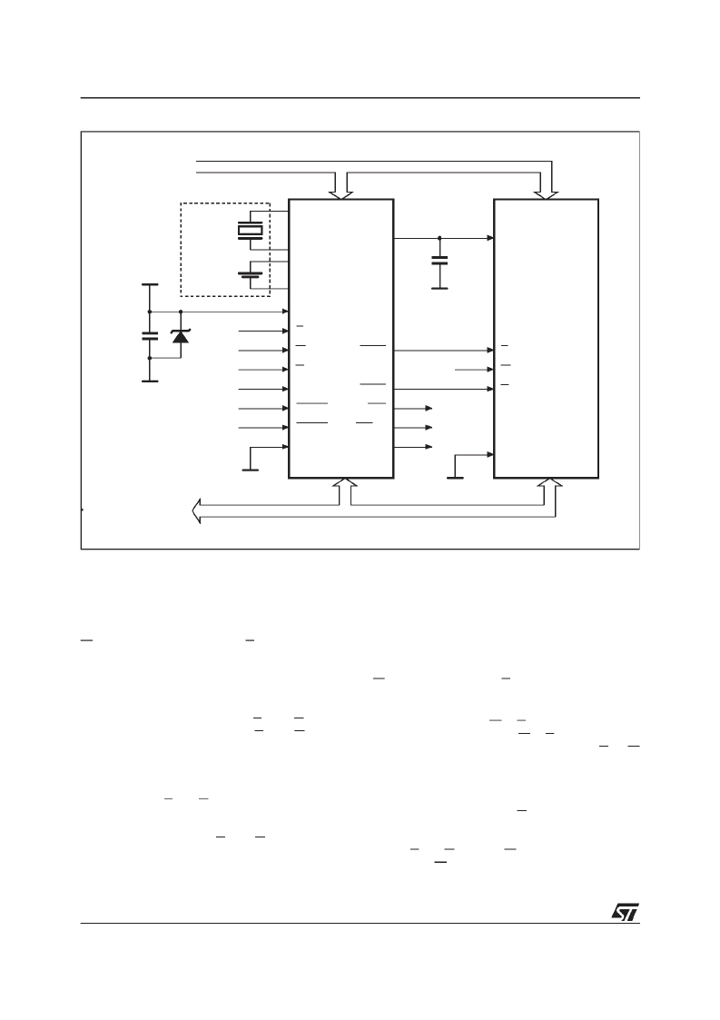
Figure 4. Hardware Hookup for SMT Chip Set
(1)
Note: 1. For pin connections, see individual data sheets for M48T201Y/V and M68Z128/W at www.st.com.
2. For 5V, M48T129Y (M48T201Y + M68Z128). For 3.3V, M48T129V (M48T201V + M68Z128W).
3. SNAPHAT Top ordered separately.
AI03632
32,768
Hz
CRYSTAL
LITHIUM
CELL
A0-A16
DQ0-DQ7
E
VCC
W
G
WDI
RSTIN1
RSTIN2
VSS
E
W
G
VCC
VSS
A0-A16
DQ0-DQ7
0.1
μ
F
0.1
μ
F
5V
ECON
GCON
RST
IRQ/FT
SQW
M48T201Y/V
(2)
M68Z128/W
(2)
VOUT
SNAPHAT
(3)
BATTERY/CRYSTAL
READ MODE
The M48T129Y/V is in the Read Mode whenever
W (Write Enable) is high and E (Chip Enable) is
low. The unique address specified by the 17 Ad-
dress Inputs defines which one of the 131,072
bytes of data is to be accessed. Valid data will be
available at the Data I/O pins within t
AVQV
(Ad-
dress Access Time) after the last address input
signal is stable, providing the E and G access
times are also satisfied. If the E and G access
times are not met, valid data will be available after
the latterof the Chip Enable Access Times (t
ELQV
)
or Output Enable Access Time (t
GLQV
).
The state of the eight three-state Data I/O signals
is controlled by E and G. If the outputs are activat-
ed before t
AVQV
, the data lines will be driven to an
indeterminate state until t
AVQV
. If the Address In-
puts are changed while E and G remain active,
output data will remain valid for t
AXQX
(Output
Data Hold Time) but will go indeterminate until the
next Address Access.
WRITE MODE
The M48T129Y/V is in the Write Mode whenever
W (Write Enable) and E (Chip Enable) are low
state after the address inputs are stable.
The start of a write is referencedfrom the latter oc-
curring falling edgeof W orE. A writeis terminated
by theearlier rising edge of W orE. The addresses
must be held valid throughout the cycle. E or W
must return high for a minimum of t
EHAX
from Chip
Enable or t
WHAX
from Write Enable prior to the ini-
tiation of another read or write cycle. Data-in must
be valid t
DVWH
prior to the end of write and remain
valid for t
WHDX
afterward. G should be kept high
during write cycles to avoid bus contention; al-
though, if the output bus has been activated by a
low on E and Ga lowon W will disable the outputs
t
WLQZ
after W falls.
相关PDF资料 |
PDF描述 |
|---|---|
| M48T129Y-85CS1 | 3.3V-5V 1 Mbit 128Kb x8 TIMEKEEPER SRAM |
| M48T129Y-85PM1 | 3.3V-5V 1 Mbit 128Kb x8 TIMEKEEPER SRAM |
| M48T129V-70CS1 | 3.3V-5V 1 Mbit 128Kb x8 TIMEKEEPER SRAM |
| M48T129V-70PM1 | 3.3V-5V 1 Mbit 128Kb x8 TIMEKEEPER SRAM |
| M48T129 | 3.3V-5V 1 Mbit 128Kb x8 TIMEKEEPER SRAM |
相关代理商/技术参数 |
参数描述 |
|---|---|
| M48T18 | 制造商:STMICROELECTRONICS 制造商全称:STMicroelectronics 功能描述:5V, 64Kbit (8 Kb x 8) TIMEKEEPER㈢ SRAM |
| M48T18-100MH1 | 功能描述:RAM其它 8KX8 TIMEKEEP 100NS RoHS:否 制造商:Freescale Semiconductor 封装:Tray |
| M48T18-100MH1E | 制造商:STMICROELECTRONICS 制造商全称:STMicroelectronics 功能描述:64 Kbit 8Kb x 8 TIMEKEEPER SRAM |
| M48T18-100MH1F | 制造商:STMICROELECTRONICS 制造商全称:STMicroelectronics 功能描述:64 Kbit 8Kb x 8 TIMEKEEPER SRAM |
| M48T18-100MH1TR | 制造商:STMICROELECTRONICS 制造商全称:STMicroelectronics 功能描述:64 Kbit 8Kb x 8 TIMEKEEPER SRAM |
发布紧急采购,3分钟左右您将得到回复。