- 您现在的位置:买卖IC网 > PDF目录359066 > M48T512Y-85PM1 (意法半导体) 3.3V-5V 4 Mbit 512Kb x8 TIMEKEEPER SRAM PDF资料下载
参数资料
| 型号: | M48T512Y-85PM1 |
| 厂商: | 意法半导体 |
| 英文描述: | 3.3V-5V 4 Mbit 512Kb x8 TIMEKEEPER SRAM |
| 中文描述: | 3.3 - 5V的4兆位的SRAM 512KB的x8计时器 |
| 文件页数: | 3/14页 |
| 文件大小: | 104K |
| 代理商: | M48T512Y-85PM1 |
3/14
M48T512Y, M48T512V
Table 3. Operating Modes
(1)
Mode
Note: 1. X = V
IH
or V
IL
.
2. See Table 7 for details.
V
CC
E
G
W
DQ0-DQ7
Power
Deselect
4.5V to 5.5V
or
3.0V to 3.6V
V
IH
V
IL
V
IL
V
IL
X
X
High Z
Standby
Write
X
V
IL
V
IH
V
IH
D
IN
D
OUT
Active
Read
V
IL
V
IH
Active
Read
High Z
Active
Deselect
V
SO
to V
PFD
(min)
(2)
≤
V
SO (2)
X
X
X
High Z
CMOS Standby
Deselect
X
X
X
High Z
Battery Back-up Mode
Table 4. AC Measurement Conditions
Note that Output Hi-Z is defined as the point where data is no longer
driven.
Input Rise and Fall Times
≤
5ns
Input Pulse Voltages
0 to 3V
Input and Output Timing Ref. Voltages
1.5V
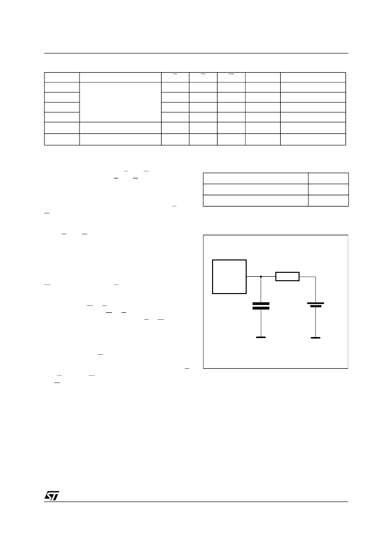
Figure 3. AC Testing Load Circuit
AI01803C
CL = 100pF
CL includes JIG capacitance
650
DEVICE
UNDER
TEST
1.75V
cess Time (t
AVQV
) after the last address input sig-
nal is stable, providing the E and G access times
are also satisfied. If the E and G access times are
not met, valid data will be available after the latter
of the Chip Enable Access Times (t
ELQV
) or Output
Enable Access Time (t
GLQV
). The state of the eight
three-state Data I/O signals is controlled by E and
G. If the outputs are activated before t
AVQV
, the
data lines will be driven to an indeterminate state
until t
AVQV
. If the Address Inputs are changed
while E and G remain active, output data will re-
main valid for Output Data Hold Time (t
AXQX
) but
will go indeterminate until the next Address Ac-
cess.
WRITE MODE
The M48T512Y/V is in the Write Mode whenever
W (Write Enable) and E (Chip Enable) are low
state after the address inputs are stable. The start
of a write is referenced from the latter occurring
falling edge of W or E. A write is terminated by the
earlier rising edge of W or E. The addresses must
be held valid throughout the cycle. E or W must re-
turn high for a minimum of t
EHAX
from Chip Enable
or t
WHAX
from Write Enable prior to the initiation of
another read or write cycle. Data-in must be valid
t
DVWH
prior to the end of write and remain valid for
t
WHDX
afterward. G should be kept high during
write cycles to avoid bus contention; although, if
the output bus has been activated by a low on E
and G a low on W will disable the outputs t
WLQZ
af-
ter W falls.
相关PDF资料 |
PDF描述 |
|---|---|
| M48T512YPM | 3.3V-5V 4 Mbit 512Kb x8 TIMEKEEPER SRAM |
| M48T513VPM | 3.3V-5V 4 Mbit 512Kb x8 TIMEKEEPER SRAM |
| M48T513V-70CS1 | 3.3V-5V 4 Mbit 512Kb x8 TIMEKEEPER SRAM |
| M48T513V-70PM1 | 3.3V-5V 4 Mbit 512Kb x8 TIMEKEEPER SRAM |
| M48T513V-85CS1 | 3.3V-5V 4 Mbit 512Kb x8 TIMEKEEPER SRAM |
相关代理商/技术参数 |
参数描述 |
|---|---|
| M48T512YPM | 制造商:STMICROELECTRONICS 制造商全称:STMicroelectronics 功能描述:3.3V-5V 4 Mbit 512Kb x8 TIMEKEEPER SRAM |
| M48T513V | 制造商:STMICROELECTRONICS 制造商全称:STMicroelectronics 功能描述:3.3V-5V 4 Mbit 512Kb x8 TIMEKEEPER SRAM |
| M48T513V-70CS1 | 制造商:STMICROELECTRONICS 制造商全称:STMicroelectronics 功能描述:3.3V-5V 4 Mbit 512Kb x8 TIMEKEEPER SRAM |
| M48T513V-70PM1 | 制造商:STMICROELECTRONICS 制造商全称:STMicroelectronics 功能描述:3.3V-5V 4 Mbit 512Kb x8 TIMEKEEPER SRAM |
| M48T513V-85CS1 | 制造商:STMICROELECTRONICS 制造商全称:STMicroelectronics 功能描述:3.3V-5V 4 Mbit 512Kb x8 TIMEKEEPER SRAM |
发布紧急采购,3分钟左右您将得到回复。