- 您现在的位置:买卖IC网 > PDF目录132964 > M48T512Y-85PM1 (STMICROELECTRONICS) REAL TIME CLOCK, PDIP32 PDF资料下载
参数资料
| 型号: | M48T512Y-85PM1 |
| 厂商: | STMICROELECTRONICS |
| 元件分类: | 时钟/数据恢复及定时提取 |
| 英文描述: | REAL TIME CLOCK, PDIP32 |
| 封装: | ROHS COMPLIANT, PLASTIC, DIP-32 |
| 文件页数: | 2/23页 |
| 文件大小: | 370K |
| 代理商: | M48T512Y-85PM1 |
Operating modes
M48T512Y, M48T512V
Doc ID 5747 Rev 6
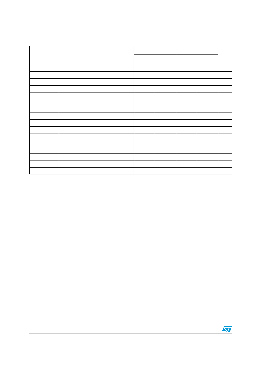
Table 4.
WRITE mode AC characteristics
2.3
Data retention mode
With valid VCC applied, the M48T512Y/V operates as a conventional BYTEWIDE static
RAM. Should the supply voltage decay, the RAM will automatically deselect, write protecting
itself when VCC falls between VPFD (max) and VPFD (min). All outputs become high
impedance and all inputs are treated as “Don't care.”
Note:
A power failure during a WRITE cycle may corrupt data at the current addressed location,
but does not jeopardize the rest of the RAM's content. At voltages below VPFD (min), the
memory will be in a write protected state, provided the VCC fall time is not less than tF. The
M48T512Y/V may respond to transient noise spikes on VCC that cross into the deselect
window during the time the device is sampling VCC.Therefore, decoupling of the power
supply lines is recommended. When VCC drops below VSO, the control circuit switches
power to the internal battery, preserving data and powering the clock. The internal energy
source will maintain data in the M48T512Y/V for an accumulated period of at least 10 years
at room temperature. As system power rises above VSO, the battery is disconnected, and
the power supply is switched to external VCC. Write protection continues until VCC reaches
VPFD (min) plus tREC (min). Normal RAM operation can resume tREC after VCC exceeds
VPFD (max). Refer to Application Note (AN1012) on the ST website for more information on
battery life.
Symbol
Parameter(1)
1.
Valid for ambient operating temperature: TA = 0 to 70 °C; VCC = 4.5 to 5.5 V or 3.0 to 3.6 V (except where noted).
M48T512Y
M48T512V
Unit
-70
-85
Min
Max
Min
Max
tAVAV
WRITE cycle time
70
85
ns
tAVWL
Address valid to WRITE enable low
0
ns
tAVEL
Address valid to chip enable low
0
ns
tWLWH
WRITE enable pulse width
50
60
ns
tELEH
Chip enable low to chip enable high
55
65
ns
tWHAX
WRITE enable high to address transition
5
ns
tEHAX
Chip enable high to address transition
10
15
ns
tDVWH
Input valid to WRITE enable high
30
35
ns
tDVEH
Input valid to chip enable high
30
35
ns
tWHDX
WRITE enable high to input transition
5
ns
tEHDX
Chip enable high to input transition
10
15
ns
tWLQZ
(2)(3)
2.
CL = 5pF.
3.
If E goes low simultaneously with W going low, the outputs remain in the high impedance state.
WRITE enable low to output Hi-Z
25
30
ns
tAVWH
Address valid to write enable high
60
70
ns
tAVEH
Address valid to chip enable high
60
70
ns
tWHQX
WRITE enable high to output transition
5
ns
相关PDF资料 |
PDF描述 |
|---|---|
| MB89202YPFV | 8-BIT, MROM, 12.5 MHz, MICROCONTROLLER, PDSO34 |
| MPC7410THX450LE | 32-BIT, 450 MHz, RISC PROCESSOR, CBGA360 |
| M48T08Y-10MH1F | 0 TIMER(S), REAL TIME CLOCK, PDSO28 |
| MK2703SILFTR | 27 MHz, OTHER CLOCK GENERATOR, PDSO8 |
| MC9S08RE16CFG | 8-BIT, FLASH, 8 MHz, MICROCONTROLLER, PQFP44 |
相关代理商/技术参数 |
参数描述 |
|---|---|
| M48T512YPM | 制造商:STMICROELECTRONICS 制造商全称:STMicroelectronics 功能描述:3.3V-5V 4 Mbit 512Kb x8 TIMEKEEPER SRAM |
| M48T513V | 制造商:STMICROELECTRONICS 制造商全称:STMicroelectronics 功能描述:3.3V-5V 4 Mbit 512Kb x8 TIMEKEEPER SRAM |
| M48T513V-70CS1 | 制造商:STMICROELECTRONICS 制造商全称:STMicroelectronics 功能描述:3.3V-5V 4 Mbit 512Kb x8 TIMEKEEPER SRAM |
| M48T513V-70PM1 | 制造商:STMICROELECTRONICS 制造商全称:STMicroelectronics 功能描述:3.3V-5V 4 Mbit 512Kb x8 TIMEKEEPER SRAM |
| M48T513V-85CS1 | 制造商:STMICROELECTRONICS 制造商全称:STMicroelectronics 功能描述:3.3V-5V 4 Mbit 512Kb x8 TIMEKEEPER SRAM |
发布紧急采购,3分钟左右您将得到回复。