- 您现在的位置:买卖IC网 > PDF目录383302 > M50FW040K5G (意法半导体) 4-Mbit (512 Kb x8, uniform block) 3-V supply firmware hub Flash memory PDF资料下载
参数资料
| 型号: | M50FW040K5G |
| 厂商: | 意法半导体 |
| 英文描述: | 4-Mbit (512 Kb x8, uniform block) 3-V supply firmware hub Flash memory |
| 中文描述: | 4兆位(512 KB的× 8,均匀块)3 - V电源供电的闪存固件枢纽 |
| 文件页数: | 32/53页 |
| 文件大小: | 278K |
| 代理商: | M50FW040K5G |
第1页第2页第3页第4页第5页第6页第7页第8页第9页第10页第11页第12页第13页第14页第15页第16页第17页第18页第19页第20页第21页第22页第23页第24页第25页第26页第27页第28页第29页第30页第31页当前第32页第33页第34页第35页第36页第37页第38页第39页第40页第41页第42页第43页第44页第45页第46页第47页第48页第49页第50页第51页第52页第53页
Firmware hub (FWH) interface Configuration Registers
M50FW040
32/53
6.7
Device Code Register
Reading the Device Code Register returns the device code for the memory, 2Ch. This
register is read-only and writing to it has no effect.
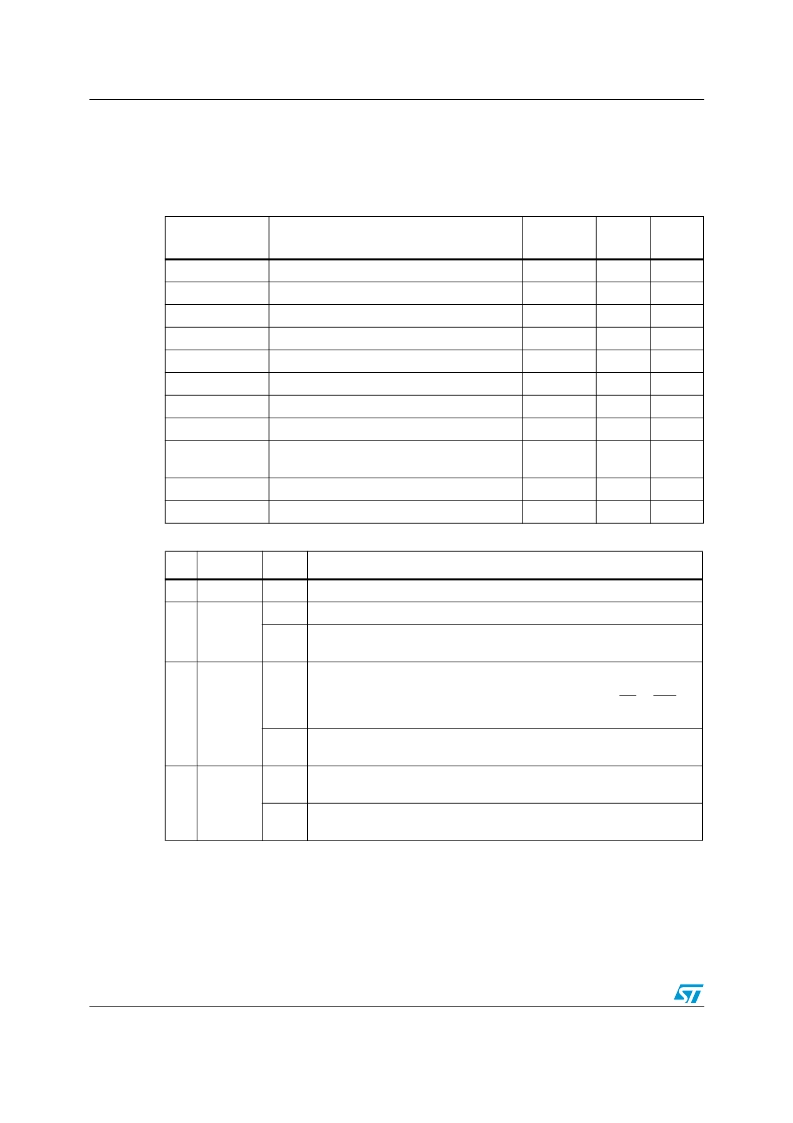
Table 9.
Table 10.
Firmware hub Configuration Register map
Mnemonic
Register Name
Memory
Address
Default
Value
Access
T_BLOCK_LK
Top Block Lock Register (Block 7)
FBF0002h
01h
R/W
T_MINUS01_LK
Top Block [-1] Lock Register (Block 6)
FBE0002h
01h
R/W
T_MINUS02_LK
Top Block [-2] Lock Register (Block 5)
FBD0002h
01h
R/W
T_MINUS03_LK
Top Block [-3] Lock Register (Block 4)
FBC0002h
01h
R/W
T_MINUS04_LK
Top Block [-4] Lock Register (Block 3)
FBB0002h
01h
R/W
T_MINUS05_LK
Top Block [-5] Lock Register (Block 2)
FBA0002h
01h
R/W
T_MINUS06_LK
Top Block [-6] Lock Register (Block 1)
FB90002h
01h
R/W
T_MINUS07_LK
Top Block [-7] Lock Register (Block 0)
FB80002h
01h
R/W
FGPI_REG
Firmware Hub (FWH) General Purpose Input
Register
FBC0100h
N/A
R
MANUF_REG
Manufacturer Code Register
FBC0000h
20h
R
DEV_REG
Device Code Register
FBC0001h
2Ch
R
Lock Register bit definitions
(1)
1.
Applies to Top Block Lock Register (T_BLOCK_LK) and Top Block [-1] Lock Register (T_MINUS01_LK) to
Top Block [-7] Lock Register (T_MINUS07_LK).
Bit
Bit name
Value
Function
7-3
Reserved
2
Read-
Lock
‘1’
Bus Read operations in this Block always return 00h.
‘0’
Bus read operations in this Block return the Memory Array contents.
(Default value).
1
Lock-
Down
‘1’
Changes to the Read-Lock bit and the Write-Lock bit cannot be
performed. Once a ‘1’ is written to the Lock-Down bit it cannot be cleared
to ‘0’; the bit is always reset to ‘0’ following a Reset (using RP or INIT) or
after power-up.
‘0’
Read-Lock and Write-Lock can be changed by writing new values to
them. (Default value).
0
Write-
Lock
‘1’
Program and Erase operations in this Block will set an error in the Status
Register. The memory contents will not be changed. (Default value).
‘0’
Program and Erase operations in this Block are executed and will modify
the Block contents.
相关PDF资料 |
PDF描述 |
|---|---|
| M50FW040K5P | 4-Mbit (512 Kb x8, uniform block) 3-V supply firmware hub Flash memory |
| M50FW040K5TG | 4-Mbit (512 Kb x8, uniform block) 3-V supply firmware hub Flash memory |
| M50FW040K5TP | 4-Mbit (512 Kb x8, uniform block) 3-V supply firmware hub Flash memory |
| M50FW040N5G | 4-Mbit (512 Kb x8, uniform block) 3-V supply firmware hub Flash memory |
| M50FW040N5P | 4-Mbit (512 Kb x8, uniform block) 3-V supply firmware hub Flash memory |
相关代理商/技术参数 |
参数描述 |
|---|---|
| M50FW040K5P | 制造商:STMICROELECTRONICS 制造商全称:STMicroelectronics 功能描述:4-Mbit (512 Kb x8, uniform block) 3-V supply firmware hub Flash memory |
| M50FW040K5T | 制造商:STMICROELECTRONICS 制造商全称:STMicroelectronics 功能描述:4 Mbit 512Kb x8, Uniform Block 3V Supply Firmware Hub Flash Memory |
| M50FW040K5TG | 功能描述:闪存 SERIAL FLASH RoHS:否 制造商:ON Semiconductor 数据总线宽度:1 bit 存储类型:Flash 存储容量:2 MB 结构:256 K x 8 定时类型: 接口类型:SPI 访问时间: 电源电压-最大:3.6 V 电源电压-最小:2.3 V 最大工作电流:15 mA 工作温度:- 40 C to + 85 C 安装风格:SMD/SMT 封装 / 箱体: 封装:Reel |
| M50FW040K5TP | 制造商:STMICROELECTRONICS 制造商全称:STMicroelectronics 功能描述:4-Mbit (512 Kb x8, uniform block) 3-V supply firmware hub Flash memory |
| M50FW040N | 制造商:STMICROELECTRONICS 制造商全称:STMicroelectronics 功能描述:4 Mbit 512Kb x8, Uniform Block 3V Supply Firmware Hub Flash Memory |
发布紧急采购,3分钟左右您将得到回复。