- 您现在的位置:买卖IC网 > PDF目录370984 > M5M5V4R08J-15 (Mitsubishi Electric Corporation) TV 37C 37#22D SKT RECP PDF资料下载
参数资料
| 型号: | M5M5V4R08J-15 |
| 厂商: | Mitsubishi Electric Corporation |
| 英文描述: | TV 37C 37#22D SKT RECP |
| 中文描述: | 4194304位(524288 - Word的8位)的CMOS静态RAM |
| 文件页数: | 2/12页 |
| 文件大小: | 56K |
| 代理商: | M5M5V4R08J-15 |
M5M5V4R08J-12,-15,-20
4194304-BIT (524288-WORD BY 8-BIT) CMOS STATIC RAM
MITSUBISHI
ELECTRIC
MITSUBISHI LSIs
2
The operation mode of the M5M5V4R08J is determined by a
combination of the device control inputs S, W and OE. Each mode
is summarized in the function table.
A write cycle is executed whenever the low level W overlaps
with the low level S. The address must be set-up before the write
cycle and must be stable during the entire cycle.
The data is latched into a cell on the trailing edge of W or S,
whichever occurs first, requiring the set-up and hold time relative
to these edge to be maintained. The output enable input OE
directly controls the output stage. Setting the OE at a high level,
the output stage is in a high impedance state, and the data bus
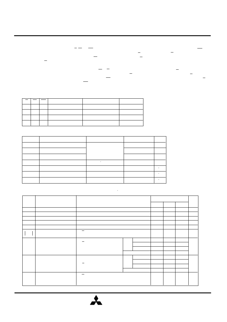
FUNCTION TABLE
contention problem in the write cycle is eliminated.
A read cycle is excuted by setting W at a high level and OE at a
low level while S are in an active state (S=L).
When setting S at high level, the chip is in a non-selectable
mode in which both reading and writing are disable. In this mode,
the output stage is in a high-impedance state, allowing OR-tie
with other chips and memory expansion by S.
Signal-S controls the power-down feature. When S goes high,
power dissapation is reduced extremely. The access time from S is
equivalent to the address access time.
FUNCTION
Icc
S
H
L
L
L
W
X
L
H
H
OE
X
X
L
H
Mode
Non selection
Write
Read
Stand by
Active
Active
Active
ABSOLUTE MAXIMUM RATINGS
DQ
High-impedance
Din
Dout
High-impedance
Operating temperature
V
cc
V
I
V
O
P
d
T
opr
T
stg(bias)
T
stg
V
V
V
mW
-2.0 ~ 4.6
1000
0 ~ 70
-10 ~ 85
-65 ~ 150
Parameter
Supply voltage
Input voltage
Output voltage
Power dissipation
Storage temperature
(bias)
Storage temperature
Symbol
Unit
Conditions
With respect to GND
Ratings
V
IH
V
IL
V
OH
V
OL
I
I
V
V
V
V
μA
Vcc+0.3
0.8
2.0
2.4
0.4
Symbol
Parameter
Max
Typ
Limits
Min
Condition
Unit
High-level input voltage
Low-level input voltage
High-level output voltage
Low-level output voltage
Input current
I
CC1
I
CC2
I
CC3
mA
mA
170
160
150
I
OZ
2
10
AC
DC
10
Active supply current
(TTL level)
Stand by current
(TTL level)
Output current in off-state
Stand by current
110
120
85
80
75
12ns cycle
15ns cycle
20ns cycle
mA
AC
DC
60
12ns cycle
15ns cycle
20ns cycle
1
-2.0 ~ VCC+0.5
-2.0 ~ VCC+0.5
C
C
C
Ta=25 C
*Pulse width
≤
20ns, In case of DC:-0.5V
DC ELECTRICAL CHARACTERISTICS
(Ta=0 ~ 70 C, Vcc=3.3V unless otherwise noted)
-0.3*
μA
I
OH
=-4mA
I
OL
= 8mA
V
I
= 0~Vcc
V
I (S)
= V
IH
V
O
= 0~Vcc
V
I (S)
= V
IL
other inputs V
IH
or V
IL
Output-open(duty 100%)
V
I (S)
=
Vcc
≥
0.2V
other inputs V
I
≤
0.2V
or V
I
≥
Vcc-0.2V
V
I (S)
= V
IH
*Pulse width
≤
20ns, in case of AC :-3.0V
相关PDF资料 |
PDF描述 |
|---|---|
| M5M5V5636GP-16 | 18874368-BIT(524288-WORD BY 36-BIT) NETWORK SRAM |
| M5M5V5636GP16 | 18874368-BIT(524288-WORD BY 36-BIT) NETWORK SRAM |
| M5M5W816TP-70HI | 8388608-BIT (524288-WORD BY 16-BIT) CMOS STATIC RAM |
| M5M5W816TP-85HI | 8388608-BIT (524288-WORD BY 16-BIT) CMOS STATIC RAM |
| M5M5W816WG-70HI | 8388608-BIT (524288-WORD BY 16-BIT) CMOS STATIC RAM |
相关代理商/技术参数 |
参数描述 |
|---|---|
| M5M5V4R08J-20 | 制造商:MITSUBISHI 制造商全称:Mitsubishi Electric Semiconductor 功能描述:4194304-BIT (524288-WORD BY 8-BIT) CMOS STATIC RAM |
| M5M5V5636GP-13 | 制造商:RENESAS 制造商全称:Renesas Technology Corp 功能描述:18874368-BIT(524288-WORD BY 36-BIT) NETWORK SRAM |
| M5M5V5636GP-13I | 制造商:RENESAS 制造商全称:Renesas Technology Corp 功能描述:18874368-BIT(524288-WORD BY 36-BIT) NETWORK SRAM |
| M5M5V5636GP16 | 制造商:MITSUBISHI 制造商全称:Mitsubishi Electric Semiconductor 功能描述:18874368-BIT(524288-WORD BY 36-BIT) NETWORK SRAM |
| M5M5V5636GP-16 | 制造商:MITSUBISHI 制造商全称:Mitsubishi Electric Semiconductor 功能描述:18874368-BIT(524288-WORD BY 36-BIT) NETWORK SRAM |
发布紧急采购,3分钟左右您将得到回复。