- 您现在的位置:买卖IC网 > PDF目录370984 > M5M5V5636GP16 (Mitsubishi Electric Corporation) 18874368-BIT(524288-WORD BY 36-BIT) NETWORK SRAM PDF资料下载
参数资料
| 型号: | M5M5V5636GP16 |
| 厂商: | Mitsubishi Electric Corporation |
| 英文描述: | 18874368-BIT(524288-WORD BY 36-BIT) NETWORK SRAM |
| 中文描述: | 18874368位(524288 - Word的36位)网络的SRAM |
| 文件页数: | 4/17页 |
| 文件大小: | 269K |
| 代理商: | M5M5V5636GP16 |
MITSUBISHI LSIs
M5M5V5636GP –16
18874368-BIT(524288-WORD BY 36-BIT) NETWORK SRAM
4
MITSUBISHI
ELECTRIC
Advanced Information
M5M5V5636GP REV.0.1
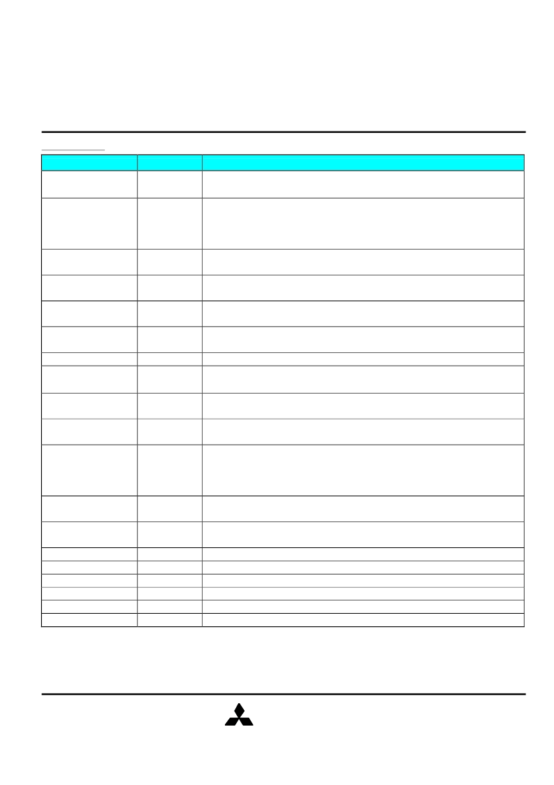
PIN FUNCTION
Pin
Name
Function
A0~A18
Synchronous
Address
Inputs
These inputs are registered and must meet the setup and hold times around the rising edge of CLK.
A0 and A1 are the two least significant bits (LSB) of the address field and set the internal burst
counter if burst is desired.
BWa#, BWb#,
BWc#, BWd#
Synchronous
Byte Write
Enables
These active LOW inputs allow individual bytes to be written when a WRITE cycle is active and
must meet the setup and hold times around the rising edge of CLK. BYTE WRITEs need to be
asserted on the same cycle as the address. BWs are associated with addresses and apply to
subsequent data. BWa# controls DQa, DQPa pins; BWb# controls DQb, DQPb pins; BWc# controls
DQc, DQPc pins; BWd# controls DQd, DQPd pins.
CLK
Clock Input
This signal registers the address, data, chip enables, byte write enables
and burst control inputs on its rising edge. All synchronous inputs must
meet setup and hold times around the clock's rising edge.
E1#
Synchronous
Chip Enable
This active LOW input is used to enable the device and is sampled only when a new external
address is loaded (ADV is LOW).
E2
Synchronous
Chip Enable
This active High input is used to enable the device and is sampled only when a new external
address is loaded (ADV is LOW). This input can be used for memory depth expansion.
E3#
Synchronous
Chip Enable
This active Low input is used to enable the device and is sampled only when a new external
address is loaded (ADV is LOW). This input can be used for memory depth expansion.
G#
Output Enable
Synchronous
Address
Advance/Load
This active LOW asynchronous input enable the data I/O output drivers.
ADV
When HIGH, this input is used to advance the internal burst counter, controlling burst access after
the external address is loaded. When HIGH, W# is ignored. A LOW on this pin permits a new
address to be loaded at CLK rising edge.
This active LOW input permits CLK to propagate throughout the device. When HIGH, the device
ignores the CLK input and effectively internally extends the previous CLK cycle. This input must
meet setup and hold times around the rising edge of CLK.
This active HIGH asynchronous input causes the device to enter a low-power standby mode in
which all data in the memory array is retained. When active, all other inputs are ignored. When this
pin is LOW or NC, the SRAM normally operates.
CKE#
Synchronous
Clock Enable
ZZ
Snooze
Enable
W#
Synchronous
Read/Write
This active input determines the cycle type when ADV is LOW. This is the only means for
determining READs and WRITEs. READ cycles may not be converted into WRITEs (and vice
versa) other than by loading a new address. A LOW on the pin permits BYTE WRITE operations
and must meet the setup and hold times around the rising edge of CLK. Full bus width WRITEs
occur if all byte write enables are LOW.
DQa,DQPa,DQb,DQPb
DQc,DQPc,DQd,DQPd
Synchronous
Data I/O
Byte “a” is DQa , DQPa pins; Byte “b” is DQb, DQPb pins; Byte “c” is DQc, DQPc pins; Byte “d” is
DQd,DQPd pins. Input data must meet setup and hold times around CLK rising edge.
LBO#
Burst Mode
Control
This DC operated pin allows the choice of either an interleaved burst or a linear burst. If this pin is
HIGH or NC, an interleaved burst occurs. When this pin is LOW, a linear burst occurs, and input
leak current to this pin.
Core Power Supply
V
DD
V
SS
V
DDQ
V
SSQ
MCH
NC
V
DD
V
SS
Core Ground
V
DDQ
I/O buffer Power supply
V
SSQ
I/O buffer Ground
Must Connect High
These pins should be connected to HIGH
No Connect
These pins are not internally connected and may be connected to ground.
相关PDF资料 |
PDF描述 |
|---|---|
| M5M5W816TP-70HI | 8388608-BIT (524288-WORD BY 16-BIT) CMOS STATIC RAM |
| M5M5W816TP-85HI | 8388608-BIT (524288-WORD BY 16-BIT) CMOS STATIC RAM |
| M5M5W816WG-70HI | 8388608-BIT (524288-WORD BY 16-BIT) CMOS STATIC RAM |
| M5M5W816WG-85HI | 8388608-BIT (524288-WORD BY 16-BIT) CMOS STATIC RAM |
| M5M5W816WG-85H | 8388608-BIT (524288-WORD BY 16-BIT) CMOS STATIC RAM |
相关代理商/技术参数 |
参数描述 |
|---|---|
| M5M5V5636GP-16 | 制造商:MITSUBISHI 制造商全称:Mitsubishi Electric Semiconductor 功能描述:18874368-BIT(524288-WORD BY 36-BIT) NETWORK SRAM |
| M5M5V5636GP-16_03 | 制造商:RENESAS 制造商全称:Renesas Technology Corp 功能描述:18874368-BIT(524288-WORD BY 36-BIT) NETWORK SRAM |
| M5M5V5636GP-16I | 制造商:Renesas Electronics Corporation 功能描述: |
| M5M5V5636GP-20 | 制造商:RENESAS 制造商全称:Renesas Technology Corp 功能描述:18874368-BIT(524288-WORD BY 36-BIT) NETWORK SRAM |
| M5M5V5636GP-22 | 制造商:RENESAS 制造商全称:Renesas Technology Corp 功能描述:18874368-BIT(524288-WORD BY 36-BIT) NETWORK SRAM |
发布紧急采购,3分钟左右您将得到回复。