- 您现在的位置:买卖IC网 > PDF目录296402 > M624-012.8M (CONNOR WINFIELD CORP) TCVCXO, CLOCK, 12.8 MHz, CMOS OUTPUT PDF资料下载
参数资料
| 型号: | M624-012.8M |
| 厂商: | CONNOR WINFIELD CORP |
| 元件分类: | XO, clock |
| 英文描述: | TCVCXO, CLOCK, 12.8 MHz, CMOS OUTPUT |
| 封装: | ROHS COMPLIANT, MINIATURE PACKAGE-8 |
| 文件页数: | 3/4页 |
| 文件大小: | 208K |
| 代理商: | M624-012.8M |
2111 Comprehensive Drive
Aurora, Illinois 60505
Phone: 630-851-4722
Fax: 630-851-5040
www.conwin.com
US Headquarters:
630-851-4722
European Headquarters:
+353-61-472221
Bulletin
Page
Revision
Date
Tx214
3of4
03
19 July 2010
Electrical Specifications for all Models
Specifications subject to change without notice. All dimensions in inches. Copyright 2008 The Connor-Winfield Corporation
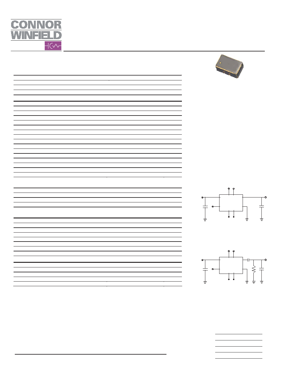
Features
LVCMOS Test Circuit
4
5
2
3
6
7
8
1
Vcc
Supply
Voltage
N/C - TCXO
VC - VCTCXO
DNC
DNC DNC
.01 uF
Bypass
Output
15 pF*
DNC
Clipped Sinewave Test Circuit
4
5
2
3
6
7
8
1
Vcc
Supply
Voltage
N/C - TCXO
VC - VCTCXO
DNC
DNC DNC
.01 uF
Bypass
Output
10 pF*
10Kohm
DNC
AC Coupling
Capacitor
DNC = Do Not Connect
* NPO Grade Component
DNC = Do Not Connect
* NPO Grade Component
M602
0806
12.8
Mhz
3.3V Operation
LVCMOS or Clipped Sinewave Output
Logic
Sub-Miniature 3.2x5.0mm SMT Package
Frequency Stabilities Available:
±
0ppm or ± . 0ppm
Temperature Ranges Available:
0to70 C
Low Power <10mA
Low Jitter <1pS RMS
Tape and Reel Packaging
RoHS Compliant / Lead Free
Recommended for new designs
±0.28ppm with STRATUM 3 Holdover,
0.5
1 0
-40 to 85 C
°
Notes
ABSOLUTE MAXIMUM RATINGS
PARAMETER
UNITS
MINIMUM
NOMINAL
MAXIMUM
UNITS
NOTE
Storage Temperature
-55
-
85
°C
Supply Voltage
(Vcc)
-0.5
-
6.0
Vdc
Input Voltage
(Vc)
-0.5
-
Vcc+0.5
Vdc
Operating Specifications
Parameter
Minimum
Nominal
Maximum
Units
Notes
TCXO Frequency Calibration @ 25
°C
-1.00
-
1.00
ppm
1
Supply Voltage Variation. (Vcc±5%)
-0.2
-
0.2
ppm
Load Coefficient, ±5%
-0.2
-
0.2
ppm
Static Temperature Hysteresis
-0.4
-
0.4
ppm
2
Aging First Year
-1.00
-
1.00
ppm
Total Frequency Tolerance
-4.60
-
4.60
ppm
3
Supply Voltage
(Vcc)
3.135
3.3
3.465
Vdc
4
Supply Current
(Icc)
-
6
10
mA
Period Jitter
-
3
5
ps rms
Integrated Phase Jitter (BW=12kHz to 20MHz)
-
0.3
1.0
ps rms
SSB Phase Noise at 10Hz offset
-
-80
-70
dBc/Hz
SSB Phase Noise at 100Hz offset
-
-110
-100
dBc/Hz
SSB Phase Noise at 1KHz offset
-
-135
-130
dBc/Hz
SSB Phase Noise at >10KHz offset
-
-150
-145
dBc/Hz
SSB Phase Noise at >100KHz offset
-
-150
dBc/Hz
Start Up Time
-
10
ms
Input Characteristics For Voltage Control (Pad 1)
Parameter
Minimum
Nominal
Maximum
Units
Notes
Control Voltage Range (Vcc = 3.3V)
(Vc)
0.3
1.65
3.0
Vdc
Frequency Tuning measured @ 25°C
±10
-
ppm
5
Linearity
±5
-
%
Slope
Positive
LVCMOS Output Characteristics
Parameter
Minimum
Nominal
Maximum
Units
Notes
LOAD
-
15
-
pF
6
Voltage
(High)
(Voh)
90%Vcc
-
Vdc
(Low)
(Vol)
-
10%Vcc
Vdc
Current
(High)
(Ioh)
-
-4
mA
(Low)
(Iol)
4
-
mA
Duty Cycle at 50% of Vcc
45
50
55
%
Rise / Fall Time 10% to 90%
-
8
ns
Clipped Sinewave Output Characteristics
Parameter
Minimum
Nominal
Maximum
Units
Notes
Load
-
7
Output Load Resistance
-
10K
-
Ohms
6
Output Load Capacitance
-
10
-
pF
6
Output Voltage
1.00
-
V pk-pk
1)
TCX O: Init ial calibr ation @ 25
°C. Specification s at t im e of shipment after 48 ho urs of o peratio n.
2)
Fr equency chang e after r ecip ro cal tem per atur e ramp ed o ver the op erating rang e. Fr equen cy m easur ed b efor e and after at 25°C .
3)
Inclu sive of calibr ation @ 25
°C, frequency vs. chan ge in temperatu re, change in supply voltage (±5%), lo ad change (± 5%), reflow
sold ering pr ocess and 20 years aging .
4)
For best in ap plication p erfor mance, car eful selection o f an ext ernal po wer so urce is cr itical. Select an exter nal reg ulat or t hat meets or
xceed s to follo wing sp ecificatio ns r egar ding voltag e reg ulatio n toleran ce, initial accur acy, temp eratur e coefficient, voltag e noise, and
lo w voltage no ise d ensity. Fa ctory T est C ond itions: Initial Accur acy ±2m v, N oise (0.1Hz to 10 KH z) 15uV p-p , Vo ltag e No ise Density
= 50nV /(Sq uare r oo t Hz), T emper atur e Coefficient < 5pp m°C .
5)
Additional pull rang es are available; please co ntact the factor y for additional inform atio n.
6)
Attention: T o achieve o ptimal freq uency st ability, and in som e cases to meet the sp ecificatio n stated o n this d ata sheet, it is r equired
that the circu it co nnected to this TCX O o utpu t must have the equ ivalent input cap acitan ce that is sp ecified b y the nominal load
capacitance. Deviation s fr om the nom ina l load capacitance will have a g radu ated effect on the stability of ap pr oximat ely 20 p pb per p F
lo ad d iffer ence.
7)
Output is DC co upled.
相关PDF资料 |
PDF描述 |
|---|---|
| M524-052.0M | TCVCXO, CLOCK, 52 MHz, CMOS OUTPUT |
| M524-FREQ | TCVCXO, CLOCK, 6.4 MHz - 52 MHz, CMOS OUTPUT |
| M514-020.0M | TCVCXO, CLOCK, 20 MHz, CMOS OUTPUT |
| M614-038.88M | TCVCXO, CLOCK, 38.88 MHz, CMOS OUTPUT |
| M52C | TRIPLE-BALANCED MIXER |
相关代理商/技术参数 |
参数描述 |
|---|---|
| M62408FP | 制造商:Panasonic Industrial Company 功能描述:IC |
| M62413FP | 制造商:MITSUBISHI 制造商全称:Mitsubishi Electric Semiconductor 功能描述:ELECTRONIC SOUND CONTROL WITH ELECTRONIC VOLUME FOR MULTIPLE SOURCES |
| M62415 | 制造商:MITSUBISHI 制造商全称:Mitsubishi Electric Semiconductor 功能描述:2CH 4 MODE PRESET EQUALIZER |
| M62415FP | 制造商:MITSUBISHI 制造商全称:Mitsubishi Electric Semiconductor 功能描述:2CH 4 MODE PRESET EQUALIZER |
| M62415P | 制造商:MITSUBISHI 制造商全称:Mitsubishi Electric Semiconductor 功能描述:2CH 4 MODE PRESET EQUALIZER |
发布紧急采购,3分钟左右您将得到回复。