- 您现在的位置:买卖IC网 > PDF目录8455 > M74VHC1GT86DTT1G (ON Semiconductor)IC GATE OR EXCL 2IN CMOS 5TSOP PDF资料下载
参数资料
| 型号: | M74VHC1GT86DTT1G |
| 厂商: | ON Semiconductor |
| 文件页数: | 1/6页 |
| 文件大小: | 0K |
| 描述: | IC GATE OR EXCL 2IN CMOS 5TSOP |
| 标准包装: | 1 |
| 系列: | 74VHC |
| 逻辑类型: | XOR(异或) |
| 电路数: | 1 |
| 输入数: | 2 |
| 电源电压: | 3 V ~ 5.5 V |
| 电流 - 静态(最大值): | 1µA |
| 输出电流高,低: | 8mA,8mA |
| 逻辑电平 - 低: | 0.53 V ~ 0.8 V |
| 逻辑电平 - 高: | 1.4 V ~ 2 V |
| 额定电压和最大 CL 时的最大传播延迟: | 8.8ns @ 4.5V ~ 5.5V,50pF |
| 工作温度: | -55°C ~ 125°C |
| 安装类型: | 表面贴装 |
| 供应商设备封装: | 5-TSOP |
| 封装/外壳: | 6-TSOP(0.059",1.50mm 宽)5 引线 |
| 包装: | 标准包装 |
| 其它名称: | M74VHC1GT86DTT1GOSDKR |
Semiconductor Components Industries, LLC, 2011
May, 2011 Rev. 16
1
Publication Order Number:
MC74VHC1GT86/D
MC74VHC1GT86
2-Input Exclusive OR Gate /
CMOS Logic Level Shifter
with LSTTLCompatible Inputs
The MC74VHC1GT86 is an advanced high speed CMOS 2input
Exclusive OR gate fabricated with silicon gate CMOS technology. It
achieves high speed operation similar to equivalent Bipolar Schottky
TTL while maintaining CMOS low power dissipation.
The internal circuit is composed of three stages, including a buffer
output which provides high noise immunity and stable output.
The device input is compatible with TTLtype input thresholds and
the output has a full 5 V CMOS level output swing. The input protection
circuitry on this device allows overvoltage tolerance on the input,
allowing the device to be used as a logiclevel translator from 3 V
CMOS logic to 5 V CMOS Logic or from 1.8 V CMOS logic to 3 V
CMOS Logic while operating at the highvoltage power supply.
The MC74VHC1GT86 input structure provides protection when
voltages up to 7 V are applied, regardless of the supply voltage. This
allows the MC74VHC1GT86 to be used to interface 5 V circuits to
3 V circuits. The output structures also provide protection when
VCC = 0 V. These input and output structures help prevent device
destruction caused by supply voltage input/output voltage mismatch,
battery backup, hot insertion, etc.
Features
High Speed: tPD = 4.8 ns (Typ) at VCC = 5 V
Low Power Dissipation: ICC = 1 mA (Max) at TA = 25°C
TTLCompatible Inputs: VIL = 0.8 V; VIH = 2 V
CMOSCompatible Outputs: VOH > 0.8 VCC; VOL < 0.1 VCC @Load
Power Down Protection Provided on Inputs and Outputs
Balanced Propagation Delays
Pin and Function Compatible with Other Standard Logic Families
Chip Complexity: FETs = 83; Equivalent Gates = 16
These Devices are PbFree and are RoHS Compliant
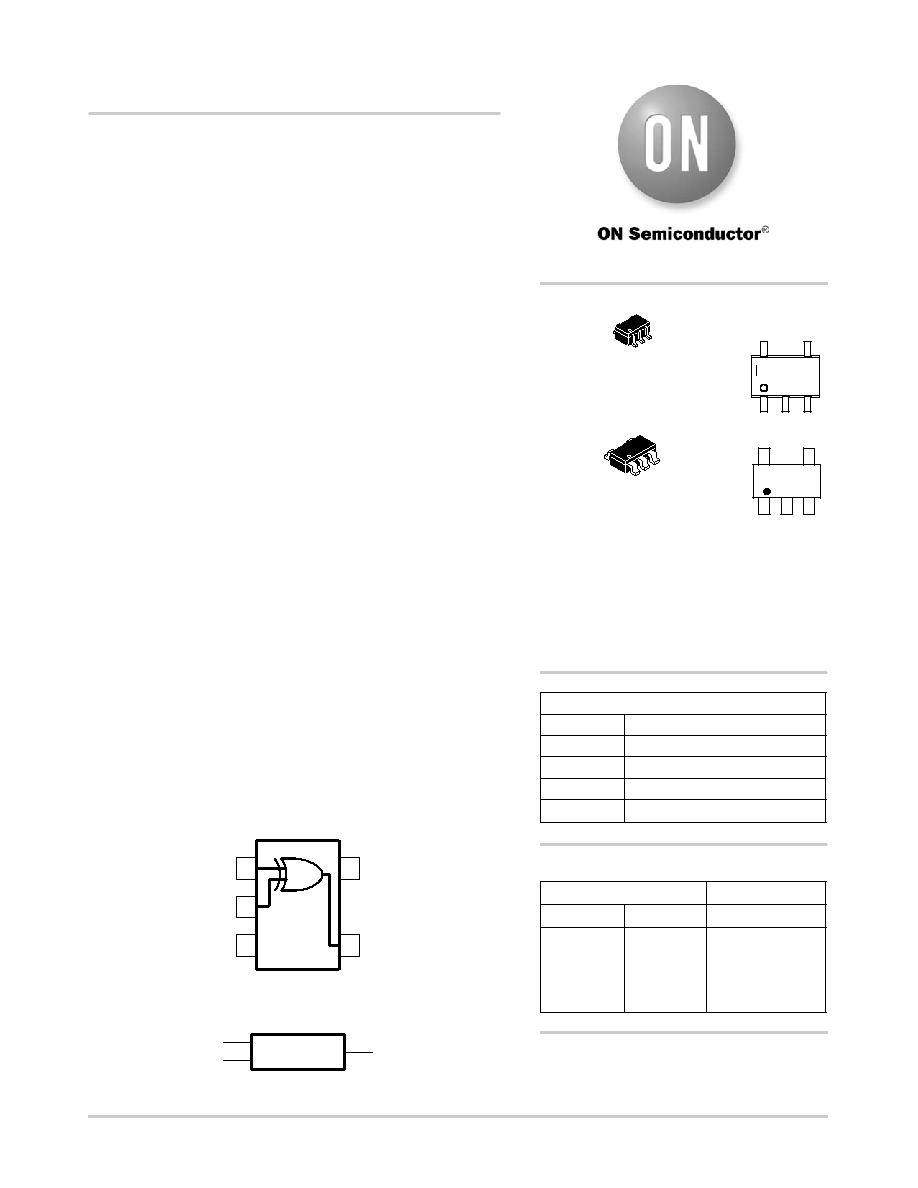
Figure 1. Pinout (Top View)
IN A
OUT Y
= 1
IN B
VCC
IN B
IN A
OUT Y
GND
Figure 2. Logic Symbol
1
2
3
4
5
http://onsemi.com
MARKING
DIAGRAMS
PIN ASSIGNMENT
1
2
3
GND
IN B
IN A
4
5VCC
OUT Y
L
H
L
H
L
H
FUNCTION TABLE
Inputs
Output
AB
L
H
L
Y
See detailed ordering and shipping information in the package
dimensions section on page 4 of this data sheet.
ORDERING INFORMATION
VM
= Device Code
M
= Date Code*
G
= PbFree Package
1
5
VM M G
G
SC88A / SOT353 / SC70
DF SUFFIX
CASE 419A
TSOP5 / SOT23 / SC59
DT SUFFIX
CASE 483
1
5
1
5
*Date Code orientation and/or position may vary
depending upon manufacturing location.
(Note: Microdot may be in either location)
1
5
VM M G
G
M
相关PDF资料 |
PDF描述 |
|---|---|
| VE-B42-MU-F4 | CONVERTER MOD DC/DC 15V 200W |
| 11 | CONN JACK PHONE 1/4" 2POS OPEN |
| VE-B41-MU-F1 | CONVERTER MOD DC/DC 12V 200W |
| 112AX | CONN JACK PHONE 1/4" 2POS CLOSED |
| VE-B13-MU-F2 | CONVERTER MOD DC/DC 24V 200W |
相关代理商/技术参数 |
参数描述 |
|---|---|
| M74VHC1GU04DFT1G | 功能描述:变换器 2-5.5V Single Unbuffered RoHS:否 制造商:NXP Semiconductors 电路数量:6 逻辑系列:74ABT 逻辑类型:BiCMOS 高电平输出电流:- 15 mA 低电平输出电流:20 mA 传播延迟时间:2.2 ns 电源电压-最大:5.5 V 电源电压-最小:4.5 V 最大工作温度:+ 85 C 最小工作温度:- 40 C 工作温度范围: 封装 / 箱体:DIP-14 封装:Tube |
| M74VHC1GU04DFT2G | 功能描述:变换器 2-5.5V Single Unbuffered RoHS:否 制造商:NXP Semiconductors 电路数量:6 逻辑系列:74ABT 逻辑类型:BiCMOS 高电平输出电流:- 15 mA 低电平输出电流:20 mA 传播延迟时间:2.2 ns 电源电压-最大:5.5 V 电源电压-最小:4.5 V 最大工作温度:+ 85 C 最小工作温度:- 40 C 工作温度范围: 封装 / 箱体:DIP-14 封装:Tube |
| M74VHC1GU04DFT2H | 制造商:Rochester Electronics LLC 功能描述: 制造商:ON Semiconductor 功能描述: |
| M74VHC1GU04DTT1G | 功能描述:变换器 2-5.5V Single Unbuffered RoHS:否 制造商:NXP Semiconductors 电路数量:6 逻辑系列:74ABT 逻辑类型:BiCMOS 高电平输出电流:- 15 mA 低电平输出电流:20 mA 传播延迟时间:2.2 ns 电源电压-最大:5.5 V 电源电压-最小:4.5 V 最大工作温度:+ 85 C 最小工作温度:- 40 C 工作温度范围: 封装 / 箱体:DIP-14 封装:Tube |
| M74VHC594RMTR | 制造商:STMICROELECTRONICS 制造商全称:STMicroelectronics 功能描述:8 BIT SHIFT REGISTER WITH OUTPUT REGISTER |
发布紧急采购,3分钟左右您将得到回复。