- 您现在的位置:买卖IC网 > PDF目录45052 > M8803F2Y-90K1 (STMICROELECTRONICS) 1M X 1 FLASH, 27 I/O, PIA-GENERAL PURPOSE, PQCC52 PDF资料下载
参数资料
| 型号: | M8803F2Y-90K1 |
| 厂商: | STMICROELECTRONICS |
| 元件分类: | 微控制器/微处理器 |
| 英文描述: | 1M X 1 FLASH, 27 I/O, PIA-GENERAL PURPOSE, PQCC52 |
| 封装: | PLASTIC, LCC-52 |
| 文件页数: | 15/85页 |
| 文件大小: | 601K |
| 代理商: | M8803F2Y-90K1 |
第1页第2页第3页第4页第5页第6页第7页第8页第9页第10页第11页第12页第13页第14页当前第15页第16页第17页第18页第19页第20页第21页第22页第23页第24页第25页第26页第27页第28页第29页第30页第31页第32页第33页第34页第35页第36页第37页第38页第39页第40页第41页第42页第43页第44页第45页第46页第47页第48页第49页第50页第51页第52页第53页第54页第55页第56页第57页第58页第59页第60页第61页第62页第63页第64页第65页第66页第67页第68页第69页第70页第71页第72页第73页第74页第75页第76页第77页第78页第79页第80页第81页第82页第83页第84页第85页
M88 FAMILY
22/85
Memory Select Configur ation for MCUs with
Separate Program and Data Spaces
The
8031
and
compatible
family
of
microcontrollers,
which includes
the
80C51,
80C151, 80C251, and 80C51XA, have separate
address spaces for code memory (selected using
PSEN) and data memory (selected using RD). Any
of
the
memories
within
the
M88x3Fxx
FLASH+PSD can reside in either space or both
spaces. This is controlled through manipulation of
the VM register that resides in the PSD’s CSIOP
space.
The VM register is set using PSDsoft to have an
initial value. It can subsequently be changed by
the microcontroller so that memory mapping can
be changed on-the-fly.
For example, I may wish to have SRAM and Flash
in Data Space at boot, and EEPROM in Program
Space at boot, and later swap EEPROM and
Flash. This is easily done with the VM register by
using PSDsoft Configuration to configure it for
boot up and having the microcontroller change it
when desired.
Table 15 describes the VM Register.
Configurati on Modes for MCUs with Separate
Program and Data Spaces
Separate Space Modes
Code memory space is separated from data
memory space. For example, the PSEN signal is
used to access the program code from the Flash
Memory, while the RD signal is used to access
data from the EEPROM, SRAM and I/O Ports.
This configuration requires the VM register to be
set to 0Ch.
Combined Space Modes
The program and data memory spaces are
combined into one space that allows the main
Flash Memory, EEPROM, and SRAM to be
accessed by either PSEN or RD. For example, to
configure the main Flash memory in combined
space mode, bits 2 and 4 of the VM register are set
to “1”.
Mixed Modes
This allows individual Flash memory or EEPROM
sectors
with
overlapping
addresses
to
be
configured in either Data Space or Program
Space. Flash memory or EEPROM sector select
signals must be qualified with the RD input in the
FS0-FS7 or EES0-EES3 equations.
An active RD will select memory sectors in the
Data Space and disable the sectors that are in the
Program Space. For memory sectors that reside in
Data Space, the access time is calculated from RD
valid to data valid. This mode is set automatically
by PSDsoft whenever the RD signal is included in
the memory sector chip select equations.
80C31 Memory Map Example
In this example, the PSD Memory will be
configured as shown in Figure 10.
t Flash Memory Sectors FS0-1 will be mapped
from 8000h-FFFFh in the Combined Space Mode
(in both Program Space and Data Space). Bits 2
and 4 of the VM Register are set to 1.
Table 15. VM Register
Bit 7
PIO_EN
Bit 6
Bit 5
Bit 4
FL_Data
Bit 3
EE_Data
Bit 2
FL_Code
Bit 1
EE_Code
Bit 0
SRAM_Code
0 = disable
PIO mode
not used
0= RD
can’t
access
Flash
0= RD
can’t
access
EEPROM/
Boot Flash
0 = PSEN
can’t
access
Flash
0 = PSEN
can’t
access
EEPROM/
Boot Flash
0 = PSEN
can’t
access
SRAM
1= enable
PIO mode
not used
1= RD
access
Flash
1= RD
access
EEPROM/
Boot Flash
1 = PSEN
access
Flash
1 = PSEN
access
EEPROM/
Boot Flash
1 = PSEN
access
SRAM
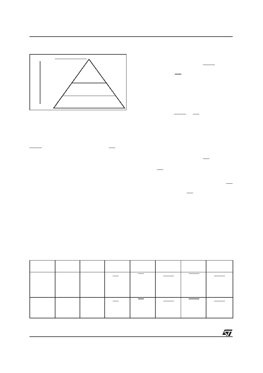
Figu re 9. Priori ty Level of Memory and I/O
Components
Level 1
SRAM, I /O, or
Peripheral I/O
Level 2
EEPROM/ Flash Boot
Memory
Highest Priority
Lowest Priority
Level 3
Flash Memory
AI02867
相关PDF资料 |
PDF描述 |
|---|---|
| M8803F3Y-90T1T | 1M X 1 FLASH, 27 I/O, PIA-GENERAL PURPOSE, PQFP52 |
| M8803F2W-15T1T | 1M X 1 FLASH, 27 I/O, PIA-GENERAL PURPOSE, PQFP52 |
| M8813F2W-15K1 | 128K X 8 FLASH, 27 I/O, PIA-GENERAL PURPOSE, PQCC52 |
| M8813F3W-15T1 | 1M X 1 FLASH, 27 I/O, PIA-GENERAL PURPOSE, PQFP52 |
| M8803F2Y-90T1 | 1M X 1 FLASH, 27 I/O, PIA-GENERAL PURPOSE, PQFP52 |
相关代理商/技术参数 |
参数描述 |
|---|---|
| M8805/100-007 | 制造商:OTTO Engineering Inc 功能描述:M8805/100-007 |
| M8805/100-009 | 制造商:OTTO Engineering Inc 功能描述:M8805/100-009 |
| M8805/100-010 | 制造商:OTTO Engineering Inc 功能描述:M8805/100-010 |
| M8805/100-015 | 制造商:OTTO Engineering Inc 功能描述:M8805/100-015 |
| M8805/100-016 | 制造商:OTTO Engineering Inc 功能描述:M8805/100-016 |
发布紧急采购,3分钟左右您将得到回复。