- 您现在的位置:买卖IC网 > PDF目录80460 > M8913F1Y-15K1 (STMICROELECTRONICS) 128K X 8 FLASH, 27 I/O, PIA-GENERAL PURPOSE, PQCC52 PDF资料下载
参数资料
| 型号: | M8913F1Y-15K1 |
| 厂商: | STMICROELECTRONICS |
| 元件分类: | 微控制器/微处理器 |
| 英文描述: | 128K X 8 FLASH, 27 I/O, PIA-GENERAL PURPOSE, PQCC52 |
| 封装: | PLASTIC, LCC-52 |
| 文件页数: | 5/7页 |
| 文件大小: | 52K |
| 代理商: | M8913F1Y-15K1 |
5/7
M89 FAMILY
erased without the use of the MCU. The primary
Flash memory can also be programmed in-system
by
the
MCU
executing
the
programming
algorithms out of the secondary memory, or
SRAM.
The
secondary
memory
can
be
programmed the same way by executing out of the
primary Flash memory. The PLD
or other
FLASH+PSD
Configuration
blocks
can
be
programmed through the JTAG port or a device
insertion programmer. Table 5 indicates which
programming methods can program different
functional blocks of the FLASH+PSD.
Power Management Unit (PMU)
The Power Management Unit (PMU) gives the
user control of the power consumption on selected
functional blocks based on system requirements.
The PMU includes an Automatic Power-down
(APD) Unit that turns off device functions during
MCU inactivity. The APD Unit has a Power-down
mode that helps reduce power consumption.
The FLASH+PSD also has some bits that are
configured at run-time by the MCU to reduce
power consumption of the GPLD. The Turbo bit in
the PMMR0 register can be reset to 0 and the
GPLD latches its outputs and goes to sleep until
the next transition on its inputs.
Additionally, bits in the PMMR2 register can be set
by the MCU to block signals from entering the
GPLD to reduce power consumption. Please see
the full data sheet for details.
SECURITY AND NVM SECTOR PROTECTION
A security bit in the Protection Register enables
the software project, coded in the FLASH+PSD, to
be locked up. This bit is only accessible by the
system designer from the JTAG serial port, or from
a parallel insertion programmer. It cannot be
accessed from the MCU. The only way a security
bit can be cleared is to erase the entire chip.
The contents of the sectors of the primary and
secondary NVM blocks can be protected using bits
in the Protection Registers. These bits are
accessible from the MCU in the application code,
or
from
a
programmer
during
the
set-up
procedure.
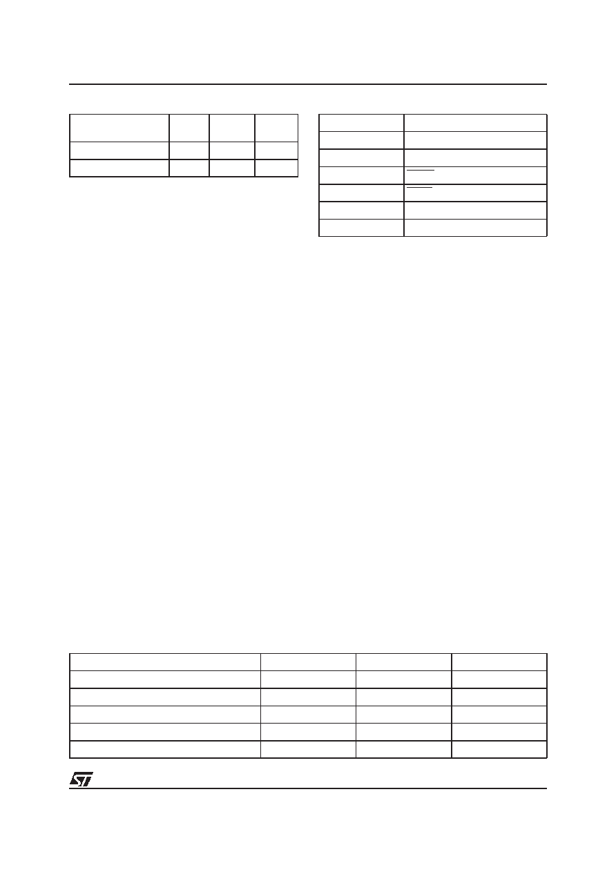
Table 3. PLD I/O
Name
Inpu ts
Outp uts
Product
Terms
Decode PLD (DPLD)
57
14
39
General PLD (GPLD)
57
19
114
Table 4. JTAG SIgnals on Port C
Port C Pins
JTAG Signal
PC0
TMS
PC1
TCK
PC3
TSTAT
PC4
TERR
PC5
TDI
PC6
TDO
Table 5. Methods of Programming Different Functional Blocks of the FLASH+PSD
Functional Block
JTAG Programming
Device Programmer
IAP
Primary Flash Memory
Yes
Secondary EEPROM or Flash memory
Yes
PLD Array (DPLD and GPLD)
Yes
No
FLASH+PSD Configuration
Yes
No
OTP Row
No
Yes
相关PDF资料 |
PDF描述 |
|---|---|
| MB90F583CAPFV | 16-BIT, FLASH, 16 MHz, MICROCONTROLLER, PQFP100 |
| MC68HC11E1CFU3R2 | 8-BIT, EEPROM, 3 MHz, MICROCONTROLLER, PQFP64 |
| MC68HC705SR3FB | 8-BIT, OTPROM, 2 MHz, MICROCONTROLLER, PQFP44 |
| MC68HC908MR8MFU | 8-BIT, FLASH, 8.2 MHz, MICROCONTROLLER, PQFP32 |
| MC6801VP1 | 8-BIT, MROM, 1 MHz, MICROCONTROLLER, PDIP40 |
相关代理商/技术参数 |
参数描述 |
|---|---|
| M8913F2W | 制造商:STMICROELECTRONICS 制造商全称:STMicroelectronics 功能描述:In-System Programmable ISP Multiple-Memory and Logic FLASHPSD Systems for MCUs |
| M8913F2Y | 制造商:STMICROELECTRONICS 制造商全称:STMicroelectronics 功能描述:In-System Programmable ISP Multiple-Memory and Logic FLASHPSD Systems for MCUs |
| M8913F2Y-90K6 | 制造商:STMicroelectronics 功能描述:FLSH+PSD 5V PLCC - Trays |
| M89141W-15K1T | 制造商:STMICROELECTRONICS 制造商全称:STMicroelectronics 功能描述:In-System Programmable ISP Multiple-Memory and Logic FLASHPSD Systems for MCUs |
| M89141W-15K6T | 制造商:STMICROELECTRONICS 制造商全称:STMicroelectronics 功能描述:In-System Programmable ISP Multiple-Memory and Logic FLASHPSD Systems for MCUs |
发布紧急采购,3分钟左右您将得到回复。