- 您现在的位置:买卖IC网 > PDF目录80516 > M926-02I622.0800 (INTEGRATED DEVICE TECHNOLOGY INC) 622.08 MHz, OTHER CLOCK GENERATOR, CQCC36 PDF资料下载
参数资料
| 型号: | M926-02I622.0800 |
| 厂商: | INTEGRATED DEVICE TECHNOLOGY INC |
| 元件分类: | 时钟产生/分配 |
| 英文描述: | 622.08 MHz, OTHER CLOCK GENERATOR, CQCC36 |
| 封装: | 9 X 9 MM, CERAMIC, LCC-36 |
| 文件页数: | 2/8页 |
| 文件大小: | 321K |
| 代理商: | M926-02I622.0800 |
M926-02 Datasheet Rev 0.7
2 of 8
Revised 30Jul2004
I n teg r at ed Circuit Systems , Inc. ● Netw o r ki ng & C o mmun ica t io ns ● ww w. icst.com ● te l (5 08 ) 8 5 2 - 54 00
M926-02
VCSO BASED CLOCK GENERATOR
Preliminar y In f o r m atio n
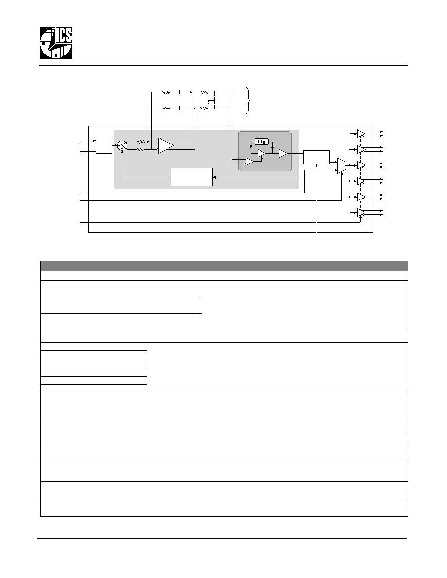
Figure 3: Detailed Block Diagram
PIN DESCRIPTIONS
Number
Name
I/O
Configuration
Description
1, 2, 3, 10, 14, 26
GND
Ground
Power supply ground connections.
4
9
OP_IN
nOP_IN
Input
External loop filter connections. See Figure 5.
5
8
nOP_OUT
OP_OUT
Output
6
7
nVC
VC
Input
11, 19, 33
VCC
Power
Power supply connection, connect to +3.3V.
12, 13
FOUT0, nFOUT0
Output
No internal terminator
Clock output pairs, differential LVPECL output
(622.08 or 155.52 MHz for the M926-02-622.0800)
15, 16
FOUT1, nFOUT1
17, 18
FOUT2, nFOUT2
20, 21
FOUT3, nFOUT3
29, 30
FOUT4, nFOUT4
31, 32
FOUT5, nFOUT5
22
FOUT_SEL
Input
Determines post-PLL divider value:
When FOUT_SEL = 0, P = 1
When FOUT_SEL = 1, P = 4
23
EN_EXT_CLK
Input
Internal pull-down
resistor1
Note 1: For typical value of internal pull-down resistor, see DC Characteristics, Pull-down on pg. 6 for typical value.
Logic 1 enables the EXT_CLK input.
Use Logic 0 for normal operation.
24
EXT_CLK
Input
External clock feed-through: 0 to 200 MHz
25
STOP
Input
Internal pull-down
resistor1
Logic 1 stops clock outputs.
Use Logic 0 for normal operation.
27
XTAL_1 / REF_IN
Input
External crystal connection. Also accepts
LVCMOS/LVTTL compatible clock source.
28
XTAL_2
Input
External crystal connection. Leave unconnected
when driving pin 27 with external clock reference.
34, 35, 36
DNC
Do Not Connect.
Internal nodes. Connection to these pins can
cause erratic device operation.
Table 2: Pin Descriptions
M926-02
VC
nVC
nOP_OUT
OP_OUT
OP_IN
nOP_IN
XTAL
OSC
1
FOUT2
nFOUT2
FOUT4
nFOUT4
FOUT3
nFOUT3
FOUT5
nFOUT5
FOUT0
nFOUT0
FOUT1
nFOUT1
FOUT_SEL
相关PDF资料 |
PDF描述 |
|---|---|
| M928-02-700.0000 | 700 MHz, OTHER CLOCK GENERATOR, CQCC36 |
| MK1411SLF | 35.46896 MHz, VIDEO CLOCK GENERATOR, PDSO8 |
| MK1726-01SLF | 32 MHz, OTHER CLOCK GENERATOR, PDSO8 |
| MK1726-02AS | 64 MHz, OTHER CLOCK GENERATOR, PDSO8 |
| MK2731-04STRLF | 36.864 MHz, VIDEO CLOCK GENERATOR, PDSO16 |
相关代理商/技术参数 |
参数描述 |
|---|---|
| M9260M | 制造商:EPCOS 制造商全称:EPCOS 功能描述:IF Filter for Audio Applications |
| M92677 | 制造商:RAYTHN 功能描述: |
| M9271 | 制造商:Tamura Corporation of America 功能描述: |
| M9278 | 制造商:Tamura Corporation of America 功能描述: |
| M9280 | 制造商:未知厂家 制造商全称:未知厂家 功能描述:VDD CONTROL |
发布紧急采购,3分钟左右您将得到回复。