- 您现在的位置:买卖IC网 > PDF目录9937 > MAX1029BEEP+T (Maxim Integrated Products)IC ADC 10BIT 300KSPS 20-QSOP PDF资料下载
参数资料
| 型号: | MAX1029BEEP+T |
| 厂商: | Maxim Integrated Products |
| 文件页数: | 3/22页 |
| 文件大小: | 0K |
| 描述: | IC ADC 10BIT 300KSPS 20-QSOP |
| 产品培训模块: | Lead (SnPb) Finish for COTS Obsolescence Mitigation Program |
| 标准包装: | 2,500 |
| 位数: | 10 |
| 采样率(每秒): | 300k |
| 数据接口: | MICROWIRE?,QSPI?,串行,SPI? |
| 转换器数目: | 1 |
| 功率耗散(最大): | 727mW |
| 电压电源: | 单电源 |
| 工作温度: | -40°C ~ 85°C |
| 安装类型: | 表面贴装 |
| 封装/外壳: | 20-SSOP(0.154",3.90mm 宽) |
| 供应商设备封装: | 20-QSOP |
| 包装: | 带卷 (TR) |
| 输入数目和类型: | 12 个单端,单极;12 个单端,双极;6 个差分,单极;6 个差分,双极 |
MAX1027/MAX1029/MAX1031
10-Bit 300ksps ADCs with FIFO,
Temp Sensor, Internal Reference
______________________________________________________________________________________
11
In differential mode, the T/H samples the difference
between two analog inputs, eliminating common-mode
DC offsets and noise. IN+ and IN- are selected from
the following pairs: AIN0/AIN1, AIN2/AIN3, AIN4/AIN5,
AIN6/AIN7, AIN8/AIN9, AIN10/AIN11, AIN12/AIN13,
and AIN14/AIN15. AIN0–AIN7 are available on the
MAX1027, MAX1029, and MAX1031. AIN8–AIN11 are
only available on the MAX1029 and MAX1031.
AIN12–AIN15 are only available on the MAX1031. See
Tables 2–5 for more details on configuring the inputs.
For the inputs that can be configured as
CNVST or an
analog input, only one can be used at a time. For the
inputs that can be configured as REF- or an analog
input, the REF- configuration excludes the analog input.
Unipolar/Bipolar
Address the unipolar and bipolar registers through the
setup register (bits 1 and 0). Program a pair of analog
channels for differential operation by writing a 1 to the
appropriate bit of the bipolar or unipolar register.
Unipolar mode sets the differential input range from 0
to VREF. A negative differential analog input in unipolar
mode causes the digital output code to be zero.
Selecting bipolar mode sets the differential input range
to ±VREF / 2. The digital output code is binary in unipo-
lar mode and two’s complement in bipolar mode (see
the transfer function graphs, Figures 8 and 9).
In single-ended mode, the MAX1027/MAX1029/
MAX1031 always operate in unipolar mode. The analog
inputs are internally referenced to GND with a full-scale
input range from 0 to VREF.
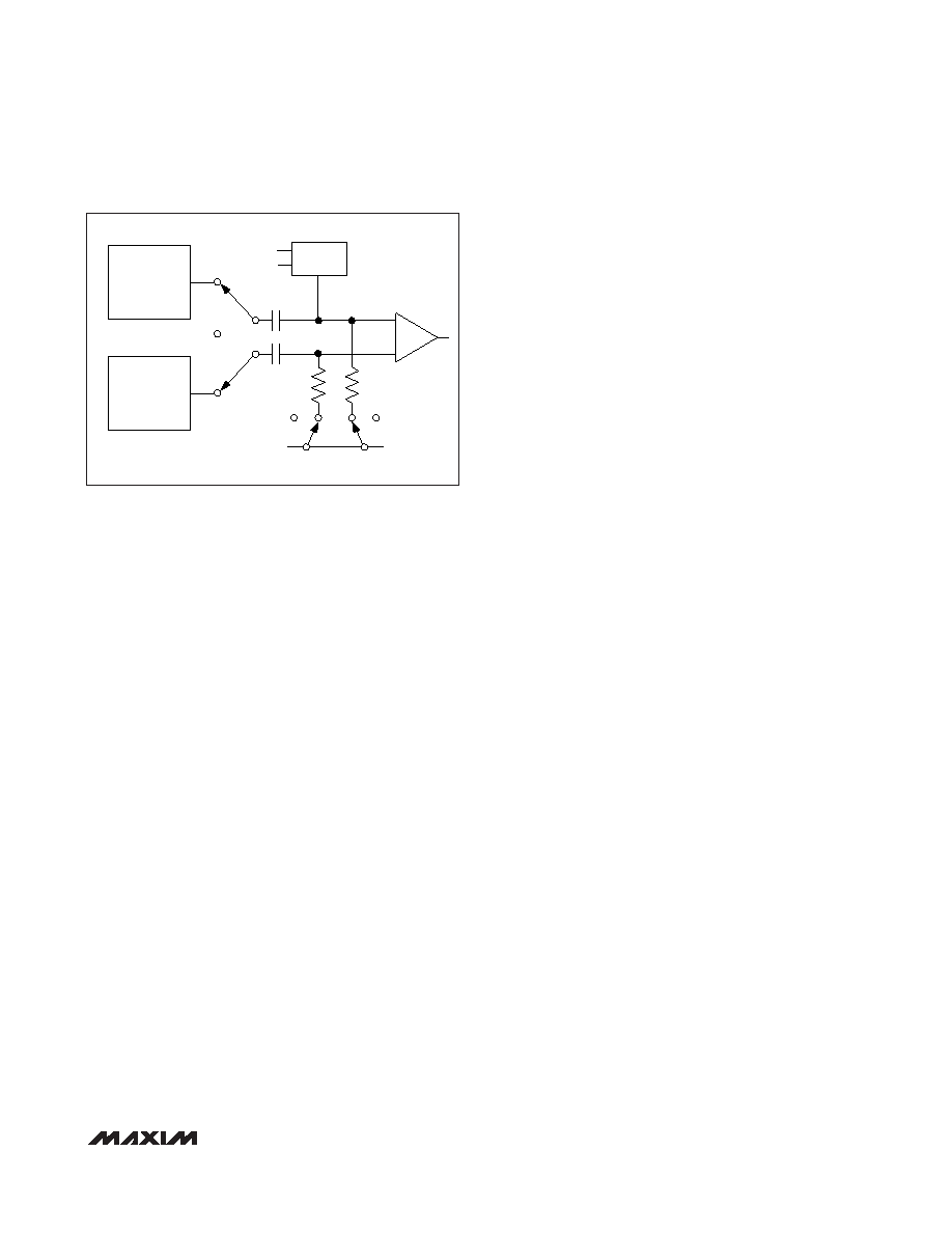
True Differential Analog Input T/H
The equivalent circuit of Figure 3 shows the
MAX1027/MAX1029/MAX1031s’ input architecture. In
track mode, a positive input capacitor is connected to
AIN0–AIN15 in single-ended mode (and AIN0, AIN2,
AIN4…AIN14 in differential mode). A negative input
capacitor is connected to GND in single-ended mode
(or AIN1, AIN3, AIN5…AIN15 in differential mode). For
external track-and-hold timing, use clock mode 01.
After the T/H enters hold mode, the difference between
the sampled positive and negative input voltages is
converted. The time required for the T/H to acquire an
input signal is determined by how quickly its input
capacitance is charged. If the input signal’s source
impedance is high, the required acquisition time
lengthens. The acquisition time, tACQ, is the maximum
time needed for a signal to be acquired, plus the power-
up time. It is calculated by the following equation:
where RIN = 1.5k
Ω, RS is the source impedance of the
input signal, and tPWR = 1μs, the power-up time of the
device. The varying power-up times are detailed in the
explanation of the clock mode conversions.
tACQ is never less than 1.4μs, and any source imped-
ance below 300
Ω does not significantly affect the
ADC’s AC performance. A high-impedance source can
be accommodated either by lengthening tACQ or by
placing a 1μF capacitor between the positive and neg-
ative analog inputs.
Internal FIFO
The MAX1027/MAX1029/MAX1031 contain a FIFO
buffer that can hold up to 16 ADC results plus one tem-
perature result. This allows the ADC to handle multiple
internally clocked conversions and a temperature mea-
surement, without tying up the serial bus.
If the FIFO is filled and further conversions are request-
ed without reading from the FIFO, the oldest ADC
results are overwritten by the new ADC results. Each
result contains 2 bytes, with the MSB preceded by four
leading zeros and the LSB followed by two sub-bits.
After each falling edge of
CS, the oldest available byte
of data is available at DOUT, MSB first. When the FIFO
is empty, DOUT is zero.
The first 2 bytes of data read out after a temperature
measurement always contain the temperature result
preceded by four leading zeros, MSB first. If another
tx R
R
x
pF
t
ACQ
S
IN
PWR
=+
()
+
924
+
-
HOLD
CIN+
REF
GND
DAC
CIN-
VDD/2
COMPARATOR
AIN0-AIN15
(SINGLE ENDED);
AIN0, AIN2,
AIN4…AIN14
(DIFFERENTIAL)
GND
(SINGLE ENDED);
AIN1, AIN3,
AIN5…AIN15
(DIFFERENTIAL)
HOLD
Figure 3. Equivalent Input Circuit
相关PDF资料 |
PDF描述 |
|---|---|
| D38999/20WG41SB | CONN RCPT 41POS WALL MNT W/SCKT |
| VI-J1B-MW-B1 | CONVERTER MOD DC/DC 95V 100W |
| IDT723634L12PF | IC FIFO SYNC 512X36X2 128QFP |
| MS27468T19B32SD | CONN RCPT 32POS JAM NUT W/SCKT |
| MAX1028BEEP+T | IC ADC 10BIT 300KSPS 20-QSOP |
相关代理商/技术参数 |
参数描述 |
|---|---|
| MAX1030 | 制造商:MAXIM 制造商全称:Maxim Integrated Products 功能描述:10-Bit 300ksps ADCs with FIFO, Temp Sensor, Internal Reference |
| MAX1030ACEG-T | 制造商:MAXIM 制造商全称:Maxim Integrated Products 功能描述:10-Bit 300ksps ADCs with FIFO, Temp Sensor, Internal Reference |
| MAX1030AEEG-T | 制造商:MAXIM 制造商全称:Maxim Integrated Products 功能描述:10-Bit 300ksps ADCs with FIFO, Temp Sensor, Internal Reference |
| MAX1030BCEG | 功能描述:模数转换器 - ADC RoHS:否 制造商:Texas Instruments 通道数量:2 结构:Sigma-Delta 转换速率:125 SPs to 8 KSPs 分辨率:24 bit 输入类型:Differential 信噪比:107 dB 接口类型:SPI 工作电源电压:1.7 V to 3.6 V, 2.7 V to 5.25 V 最大工作温度:+ 85 C 安装风格:SMD/SMT 封装 / 箱体:VQFN-32 |
| MAX1030BCEG+ | 功能描述:模数转换器 - ADC 10Bit 300ksps w/FIFO Temp Sensor Int Ref RoHS:否 制造商:Texas Instruments 通道数量:2 结构:Sigma-Delta 转换速率:125 SPs to 8 KSPs 分辨率:24 bit 输入类型:Differential 信噪比:107 dB 接口类型:SPI 工作电源电压:1.7 V to 3.6 V, 2.7 V to 5.25 V 最大工作温度:+ 85 C 安装风格:SMD/SMT 封装 / 箱体:VQFN-32 |
发布紧急采购,3分钟左右您将得到回复。