- 您现在的位置:买卖IC网 > PDF目录9469 > MAX1046BETX+T (Maxim Integrated Products)IC ADC/DAC 10BIT 36-TQFN-EP PDF资料下载
参数资料
| 型号: | MAX1046BETX+T |
| 厂商: | Maxim Integrated Products |
| 文件页数: | 24/39页 |
| 文件大小: | 0K |
| 描述: | IC ADC/DAC 10BIT 36-TQFN-EP |
| 产品培训模块: | Lead (SnPb) Finish for COTS Obsolescence Mitigation Program |
| 标准包装: | 2,500 |
| 类型: | ADC,DAC |
| 分辨率(位): | 10 b |
| 采样率(每秒): | 225k |
| 数据接口: | 串行 |
| 电压电源: | 模拟和数字 |
| 电源电压: | 4.75 V ~ 5.25 V |
| 工作温度: | -40°C ~ 85°C |
| 安装类型: | 表面贴装 |
| 封装/外壳: | 36-WFQFN 裸露焊盘 |
| 供应商设备封装: | 36-TQFN 裸露焊盘(6x6) |
| 包装: | 带卷 (TR) |
第1页第2页第3页第4页第5页第6页第7页第8页第9页第10页第11页第12页第13页第14页第15页第16页第17页第18页第19页第20页第21页第22页第23页当前第24页第25页第26页第27页第28页第29页第30页第31页第32页第33页第34页第35页第36页第37页第38页第39页
MAX1040/MAX1042/MAX1046/MAX1048
10-Bit, Multichannel ADCs/DACs with FIFO,
Temperature Sensing, and GPIO Ports
30
______________________________________________________________________________________
Do not issue a second
CNVST signal before EOC goes
low; otherwise, the FIFO can be corrupted. Wait until all
conversions are complete before reading the FIFO. SPI
communications to the DAC and GPIO registers are per-
mitted during conversion. However, coupled noise may
result in degraded ADC signal-to-noise ratio (SNR).
Externally Timed Acquisitions and
Internally Timed Conversions with
CNVST
ADC Conversions in Clock Mode 01
In clock mode 01, conversions are requested one at a
time using
CNVST and performed automatically using
the internal oscillator. See Figure 7 for clock mode 01
timing after a command byte is issued.
Setting
CNVST low begins an acquisition, wakes up the
ADC, and places it in track mode. Hold
CNVST low for
at least 1.4s to complete the acquisition. If reference
mode 00 or 10 is selected, an additional 45s is
required for the internal reference to power up. If a tem-
perature measurement is being requested, reference
power-up and temperature measurement is internally
timed. In this case, hold
CNVST low for at least 40ns.
Set
CNVST high to begin a conversion. Sampling is
completed approximately 500ns after
CNVST goes
high. After the conversion is complete, the ADC shuts
down and pulls
EOC low. EOC stays low until CS or
CNVST is pulled low again. Wait until EOC goes low
before pulling
CS or CNVST low. The number of CNVST
signals must equal the number of conversions request-
ed by the scan and averaging registers to correctly
update the FIFO. Wait until all conversions are com-
plete before reading the FIFO. SPI communications to
the DAC and GPIO registers are permitted during con-
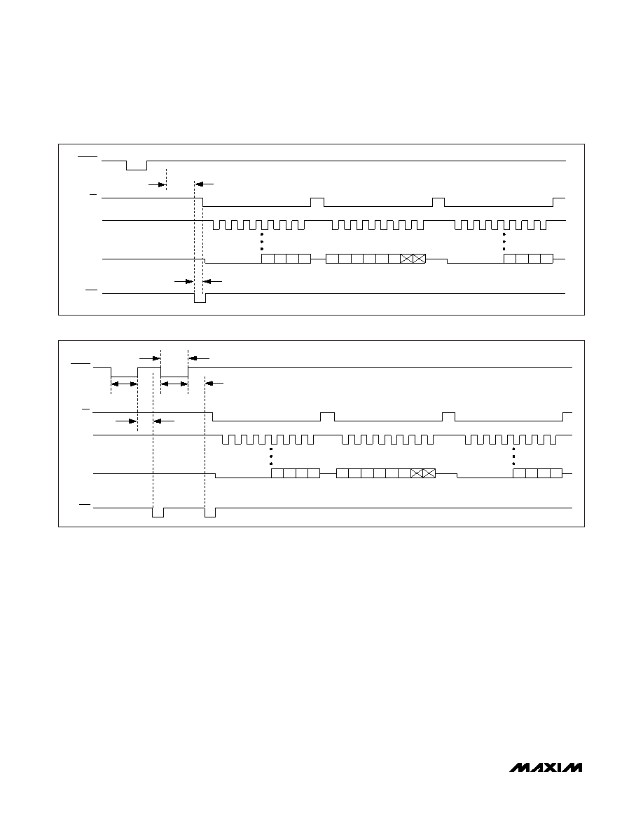
(UP TO 514 INTERNALLY CLOCKED ACQUISITIONS AND CONVERSIONS)
CS
DOUT
MSB1
tRDS
LSB1
MSB2
SCLK
CNVST
EOC
Figure 6. Clock Mode 00—After writing a command byte, set
CNVST low for at least 40ns to begin a conversion.
(CONVERSION 2)
tCSW
tDOV
(ACQUISITION 2)
(ACQUISITION 1)
(CONVERSION 1)
CS
DOUT
MSB1
LSB1
MSB2
SCLK
CNVST
EOC
Figure 7. Clock Mode 01—After writing a command byte, request multiple conversions by setting
CNVST low for each conversion.
相关PDF资料 |
PDF描述 |
|---|---|
| V300A5M300B2 | CONVERTER MOD DC/DC 5V 300W |
| VI-252-MY-S | CONVERTER MOD DC/DC 15V 50W |
| MAX1409CAP+T | IC DAS 16BIT LP 20-SSOP |
| V300A3V3M200BL3 | CONVERTER MOD DC/DC 3.3V 200W |
| VI-24K-MY-S | CONVERTER MOD DC/DC 40V 50W |
相关代理商/技术参数 |
参数描述 |
|---|---|
| MAX1048 | 制造商:MAXIM 制造商全称:Maxim Integrated Products 功能描述:10-Bit, Multichannel ADCs/DACs with FIFO, Temperature Sensing, and GPIO Ports |
| MAX1048BETX | 功能描述:ADC / DAC多通道 RoHS:否 制造商:Texas Instruments 转换速率: 分辨率:8 bit 接口类型:SPI 电压参考: 电源电压-最大:3.6 V 电源电压-最小:2 V 最大工作温度:+ 85 C 安装风格:SMD/SMT 封装 / 箱体:VQFN-40 |
| MAX1048BETX+ | 功能描述:ADC / DAC多通道 10Bit AD/DACs w/FIFO Temp Sns & GPIO Port RoHS:否 制造商:Texas Instruments 转换速率: 分辨率:8 bit 接口类型:SPI 电压参考: 电源电压-最大:3.6 V 电源电压-最小:2 V 最大工作温度:+ 85 C 安装风格:SMD/SMT 封装 / 箱体:VQFN-40 |
| MAX1048BETX+T | 功能描述:ADC / DAC多通道 10Bit AD/DACs w/FIFO Temp Sns & GPIO Port RoHS:否 制造商:Texas Instruments 转换速率: 分辨率:8 bit 接口类型:SPI 电压参考: 电源电压-最大:3.6 V 电源电压-最小:2 V 最大工作温度:+ 85 C 安装风格:SMD/SMT 封装 / 箱体:VQFN-40 |
| MAX1048BETX-T | 功能描述:ADC / DAC多通道 RoHS:否 制造商:Texas Instruments 转换速率: 分辨率:8 bit 接口类型:SPI 电压参考: 电源电压-最大:3.6 V 电源电压-最小:2 V 最大工作温度:+ 85 C 安装风格:SMD/SMT 封装 / 箱体:VQFN-40 |
发布紧急采购,3分钟左右您将得到回复。