- 您现在的位置:买卖IC网 > PDF目录9902 > MAX1067BCEE+T (Maxim Integrated Products)IC ADC 14BIT 200KSPS 16-QSOP PDF资料下载
参数资料
| 型号: | MAX1067BCEE+T |
| 厂商: | Maxim Integrated Products |
| 文件页数: | 14/30页 |
| 文件大小: | 0K |
| 描述: | IC ADC 14BIT 200KSPS 16-QSOP |
| 产品培训模块: | Lead (SnPb) Finish for COTS Obsolescence Mitigation Program |
| 标准包装: | 2,500 |
| 位数: | 14 |
| 采样率(每秒): | 200k |
| 数据接口: | MICROWIRE?,QSPI?,串行,SPI? |
| 转换器数目: | 1 |
| 功率耗散(最大): | 667mW |
| 电压电源: | 模拟和数字 |
| 工作温度: | 0°C ~ 70°C |
| 安装类型: | 表面贴装 |
| 封装/外壳: | 16-SSOP(0.154",3.90mm 宽) |
| 供应商设备封装: | 16-QSOP |
| 包装: | 带卷 (TR) |
| 输入数目和类型: | 4 个单端,单极 |
第1页第2页第3页第4页第5页第6页第7页第8页第9页第10页第11页第12页第13页当前第14页第15页第16页第17页第18页第19页第20页第21页第22页第23页第24页第25页第26页第27页第28页第29页第30页
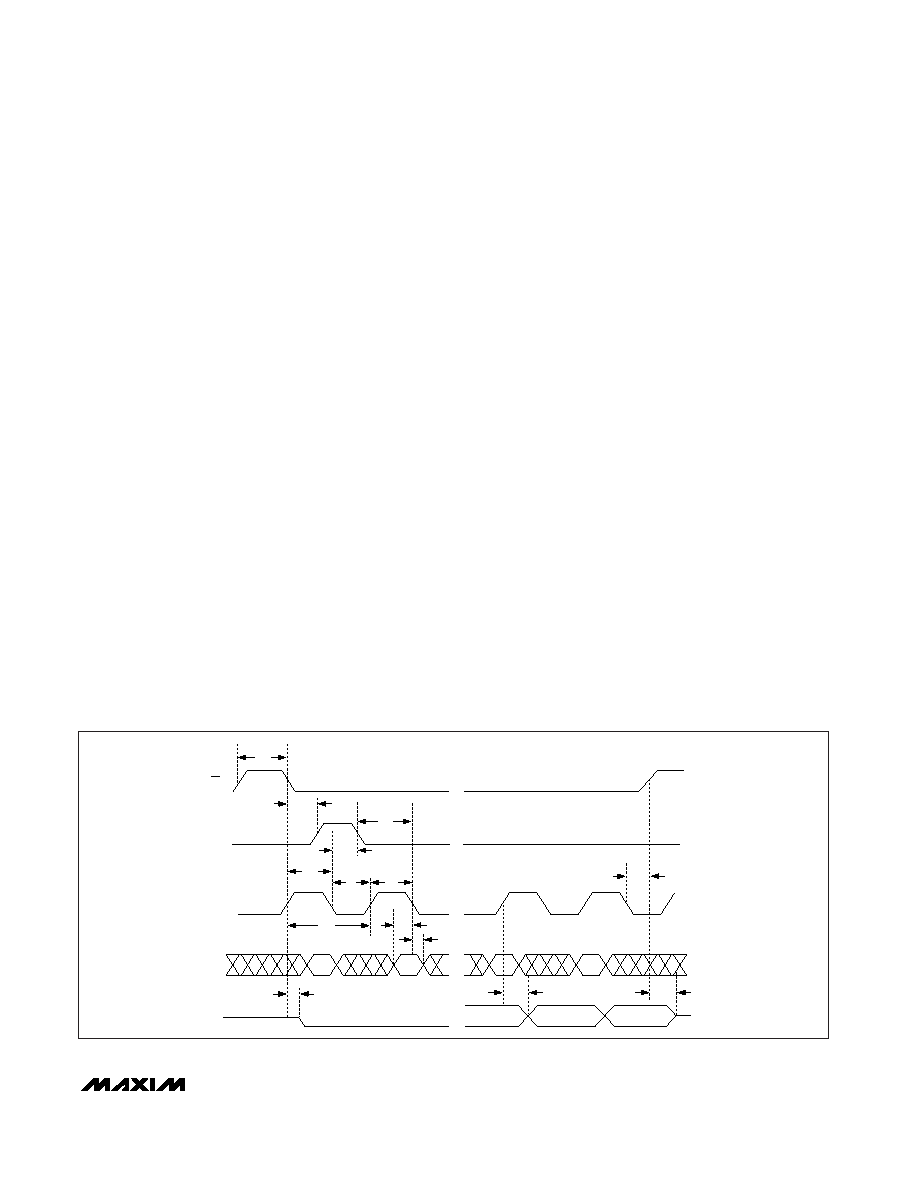
DSP 8-Bit-Wide Data-Transfer Mode (External Clock
Mode, MAX1068 Only)
Figure 16 shows the DSP-interface timing diagram.
Logic low at DSPR on the falling edge of CS enables
DSP interface mode. After the MAX1068 enters DSP
mode, CS can remain low for the duration of the con-
version process and each subsequent conversion.
Drive DSEL low to select the 8-bit data-transfer mode.
A sync pulse from the DSP at DSPR wakes the analog
circuitry and allows SCLK to clock in data (Figure 17).
The frame sync pulse alerts the MAX1068 that incom-
ing data is about to be sent to DIN. Ensure the duty
cycle on SCLK is between 45% and 55% when operat-
ing at 4.8MHz (the maximum clock frequency). For
lower clock frequencies, ensure the minimum high and
low times are at least 93ns. External clock mode con-
versions with SCLK rates less than 125kHz can reduce
accuracy due to leakage of the sampling capacitor.
The input data latches on the falling edge of SCLK. The
command/configuration/control register starts reading
data in on the falling edge of the first SCLK cycle imme-
diately following the falling edge of the frame sync
pulse and ends on the falling edge of the 8th SCLK
cycle. The MAX1068 selects the proper channel for
conversion on the falling edge of the 3rd clock cycle
and begins acquisition. Acquisition continues until the
rising edge of the 7th clock cycle. The MAX1068 sam-
ples the input on the rising edge of the 7th clock cycle.
On the rising edge of the 8th clock cycle, the MAX1068
outputs a frame sync pulse at DSPX. The frame sync
pulse alerts the DSP that the conversion results are
about to be output at DOUT (MSB first) starting on the
rising edge of the 9th clock pulse. To read the entire
conversion results, 16 SCLK cycles are needed. Extra
clock pulses, occuring after the conversion result has
been clocked out, and prior to the next rising edge of
DSPR, cause zeros to be clocked out of DOUT. The
MAX1068 external-clock, DSP 8-bit-wide data-transfer
mode requires 24 clock cycles to complete.
Begin a new conversion by sending a new frame sync
pulse to DSPR followed by new configuration data.
Send the new DSPR pulse immediately after reading
the conversion result to realize maximum throughput.
Sending a new frame sync pulse in the middle of a con-
version immediately aborts the current conversion and
begins a new one. A rising edge on CS in the middle of
a conversion aborts the current conversion and places
the MAX1068 in shutdown.
DSP 16-Bit-Wide Data-Transfer Mode (External
Clock Mode, MAX1068 Only)
Figure 16 shows the DSP-interface timing diagram. Logic
low at DSPR on the falling edge of CS enables DSP inter-
face mode. After the MAX1068 enters DSP mode, CS
can remain low for the duration of the conversion
process and each subsequent conversion. The acquisi-
tion time is extended an extra eight SCLK cycles in the
16-bit-wide data-transfer mode. Drive DSEL high to
select the 16-bit-wide data-transfer mode. A sync pulse
from the DSP at DSPR wakes the analog circuitry and
allows SCLK to clock in data (Figure 18). The frame
sync pulse also alerts the MAX1068 that incoming data
is about to be sent to DIN. Ensure the duty cycle on
SCLK is between 45% and 55% when operating at
MAX1067/MAX1068
Multichannel, 14-Bit, 200ksps Analog-to-Digital
Converters
______________________________________________________________________________________
21
CS
SCLK
DSPR
DIN
DOUT
tCSS
tCL
tDS
tDH
tDV
tCH
tDO
tTR
tFSH
tCSH
tDF
tCP
tCSW
tFSS
...
Figure 16. Detailed DSP-Interface Timing (MAX1068 Only)
相关PDF资料 |
PDF描述 |
|---|---|
| V48A28T500BG | CONVERTER MOD DC/DC 28V 500W |
| IDT72V2103L7-5BC | IC FIFO SUPERSYNCII 7-5NS 100BGA |
| MAX139CMH+TD | IC ADC 3.5 DIG W/LED DVR 44MQFP |
| IDT72V3690L7-5BBI | IC FIFO SS 32768X36 7-5N 144BGA |
| MAX1062CEUB+T | IC ADC 14BIT 200KSPS 10-UMAX |
相关代理商/技术参数 |
参数描述 |
|---|---|
| MAX1067BEEE | 功能描述:模数转换器 - ADC RoHS:否 制造商:Texas Instruments 通道数量:2 结构:Sigma-Delta 转换速率:125 SPs to 8 KSPs 分辨率:24 bit 输入类型:Differential 信噪比:107 dB 接口类型:SPI 工作电源电压:1.7 V to 3.6 V, 2.7 V to 5.25 V 最大工作温度:+ 85 C 安装风格:SMD/SMT 封装 / 箱体:VQFN-32 |
| MAX1067BEEE+ | 功能描述:模数转换器 - ADC MULTICH 200KSPS ANLG-DGTL CNVTRS RoHS:否 制造商:Texas Instruments 通道数量:2 结构:Sigma-Delta 转换速率:125 SPs to 8 KSPs 分辨率:24 bit 输入类型:Differential 信噪比:107 dB 接口类型:SPI 工作电源电压:1.7 V to 3.6 V, 2.7 V to 5.25 V 最大工作温度:+ 85 C 安装风格:SMD/SMT 封装 / 箱体:VQFN-32 |
| MAX1067BEEE+T | 制造商:Maxim Integrated Products 功能描述:- Tape and Reel 制造商:Maxim Integrated Products 功能描述:IC ADC 14BIT SRL 200KSPS 16QSOP 制造商:Maxim Integrated Products 功能描述:MULTICH 200KSPS ANLG-DGTL CNVTRS |
| MAX1067BEEE-T | 功能描述:模数转换器 - ADC RoHS:否 制造商:Texas Instruments 通道数量:2 结构:Sigma-Delta 转换速率:125 SPs to 8 KSPs 分辨率:24 bit 输入类型:Differential 信噪比:107 dB 接口类型:SPI 工作电源电压:1.7 V to 3.6 V, 2.7 V to 5.25 V 最大工作温度:+ 85 C 安装风格:SMD/SMT 封装 / 箱体:VQFN-32 |
| MAX1067CCEE | 功能描述:模数转换器 - ADC RoHS:否 制造商:Texas Instruments 通道数量:2 结构:Sigma-Delta 转换速率:125 SPs to 8 KSPs 分辨率:24 bit 输入类型:Differential 信噪比:107 dB 接口类型:SPI 工作电源电压:1.7 V to 3.6 V, 2.7 V to 5.25 V 最大工作温度:+ 85 C 安装风格:SMD/SMT 封装 / 箱体:VQFN-32 |
发布紧急采购,3分钟左右您将得到回复。