- 您现在的位置:买卖IC网 > PDF目录9749 > MAX1071CTC+T (Maxim Integrated Products)IC ADC 10BIT 1.5MSPS 12-TQFN PDF资料下载
参数资料
| 型号: | MAX1071CTC+T |
| 厂商: | Maxim Integrated Products |
| 文件页数: | 18/18页 |
| 文件大小: | 0K |
| 描述: | IC ADC 10BIT 1.5MSPS 12-TQFN |
| 标准包装: | 2,500 |
| 位数: | 10 |
| 采样率(每秒): | 1.5M |
| 数据接口: | MICROWIRE?,QSPI?,串行,SPI? |
| 转换器数目: | 1 |
| 功率耗散(最大): | 18mW |
| 电压电源: | 单电源 |
| 工作温度: | 0°C ~ 70°C |
| 安装类型: | 表面贴装 |
| 封装/外壳: | 12-WQFN 裸露焊盘 |
| 供应商设备封装: | 12-TQFN-EP(4x4) |
| 包装: | 带卷 (TR) |
| 输入数目和类型: | 1 个差分,双极 |
MAX1070/MAX1071
1.5Msps, Single-Supply, Low-Power,
True-Differential, 10-Bit ADCs
_______________________________________________________________________________________
9
Serial Interface
Initialization After Power-Up
and Starting a Conversion
Upon initial power-up, the MAX1070/MAX1071 require a
complete conversion cycle to initialize the internal cali-
bration. Following this initial conversion, the part is ready
for normal operation. This initialization is only required
after a hardware power-up sequence and is not required
after exiting partial or full power-down mode.
To start a conversion, pull CNVST low. At CNVST’s
falling edge, the T/H enters its hold mode and a con-
version is initiated. SCLK runs the conversion and the
data can then be shifted out serially on DOUT.
Timing and Control
Conversion-start and data-read operations are con-
trolled by the CNVST and SCLK digital inputs. Figures
1 and 5 show timing diagrams, which outline the serial-
interface operation.
A CNVST falling edge initiates a conversion sequence:
the T/H stage holds the input voltage, the ADC begins
to convert, and DOUT changes from high impedance
to logic low. SCLK is used to drive the conversion
process, and it shifts data out as each bit of the con-
version is determined.
SCLK begins shifting out the data after the 4th rising
edge of SCLK. DOUT transitions tDOUT after each
SCLK’s rising edge and remains valid 4ns (tDHOLD)
after the next rising edge. The 4th rising clock edge
produces the MSB of the conversion at DOUT, and the
MSB remains valid 4ns after the 5th rising edge. Since
there are 10 data bits, 2 sub-bits (S1 and S0), and 3
leading zeros, at least 16 rising clock edges are need-
ed to shift out these bits. For continuous operation, pull
CNVST high between the 14th and the 16th SCLK ris-
ing edges. If CNVST stays low after the falling edge of
the 16th SCLK cycle, the DOUT line goes to a high-
impedance state on either CNVST’s rising edge or the
next SCLK’s rising edge.
Partial Power-Down and
Full Power-Down Modes
Power consumption can be reduced significantly by
placing the MAX1070/MAX1071 in either partial power-
down mode or full power-down mode. Partial power-
down mode is ideal for infrequent data sampling and
fast wake-up time applications. Pull CNVST high after
the 3rd SCLK rising edge and before the 14th SCLK
rising edge to enter and stay in partial power-down
mode (see Figure 6). This reduces the supply current
to 1mA. Drive CNVST low and allow at least 14 SCLK
cycles to elapse before driving CNVST high to exit par-
tial power-down mode.
Full power-down mode is ideal for infrequent data sam-
pling and very low supply-current applications. The
MAX1070/MAX1071 have to be in partial power-down
mode in order to enter full power-down mode. Perform the
SCLK/CNVST sequence described above to enter partial
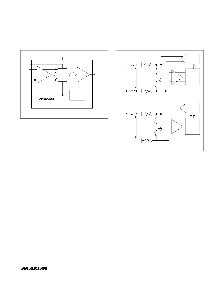
RGND
AIN+
GND
DOUT
SCLK
CNVST
CONTROL
LOGIC AND
TIMING
AIN-
VL
VDD
REF
10-BIT
SAR
ADC
MAX1070
MAX1071
T/H
OUTPUT
BUFFER
Figure 3. Functional Diagram
CIN+
RIN+
RIN-
CIN-
VAZ
AIN+
AIN-
CONTROL
LOGIC
CAPACITIVE
DAC
COMP
ACQUISITION MODE
CIN+
RIN+
RIN-
CIN-
VAZ
AIN+
AIN-
CONTROL
LOGIC
CAPACITIVE
DAC
COMP
HOLD CONVERSION MODE
Figure 4. Equivalent Input Circuit
相关PDF资料 |
PDF描述 |
|---|---|
| VE-B1X-IV-B1 | CONVERTER MOD DC/DC 5.2V 150W |
| VI-B41-MW-F4 | CONVERTER MOD DC/DC 12V 100W |
| MAX1076CTC+T | IC ADC 10BIT 1.8MSPS 12-TQFN |
| VI-2TM-MX-F3 | CONVERTER MOD DC/DC 10V 75W |
| VI-2TM-MX-F2 | CONVERTER MOD DC/DC 10V 75W |
相关代理商/技术参数 |
参数描述 |
|---|---|
| MAX1071ETC | 功能描述:模数转换器 - ADC RoHS:否 制造商:Texas Instruments 通道数量:2 结构:Sigma-Delta 转换速率:125 SPs to 8 KSPs 分辨率:24 bit 输入类型:Differential 信噪比:107 dB 接口类型:SPI 工作电源电压:1.7 V to 3.6 V, 2.7 V to 5.25 V 最大工作温度:+ 85 C 安装风格:SMD/SMT 封装 / 箱体:VQFN-32 |
| MAX1071ETC+ | 功能描述:模数转换器 - ADC 10Bit 1.5Msps Single Sply True Diff RoHS:否 制造商:Texas Instruments 通道数量:2 结构:Sigma-Delta 转换速率:125 SPs to 8 KSPs 分辨率:24 bit 输入类型:Differential 信噪比:107 dB 接口类型:SPI 工作电源电压:1.7 V to 3.6 V, 2.7 V to 5.25 V 最大工作温度:+ 85 C 安装风格:SMD/SMT 封装 / 箱体:VQFN-32 |
| MAX1071ETC+T | 功能描述:模数转换器 - ADC 10Bit 1.5Msps Single Sply True Diff RoHS:否 制造商:Texas Instruments 通道数量:2 结构:Sigma-Delta 转换速率:125 SPs to 8 KSPs 分辨率:24 bit 输入类型:Differential 信噪比:107 dB 接口类型:SPI 工作电源电压:1.7 V to 3.6 V, 2.7 V to 5.25 V 最大工作温度:+ 85 C 安装风格:SMD/SMT 封装 / 箱体:VQFN-32 |
| MAX1071ETC-T | 功能描述:模数转换器 - ADC RoHS:否 制造商:Texas Instruments 通道数量:2 结构:Sigma-Delta 转换速率:125 SPs to 8 KSPs 分辨率:24 bit 输入类型:Differential 信噪比:107 dB 接口类型:SPI 工作电源电压:1.7 V to 3.6 V, 2.7 V to 5.25 V 最大工作温度:+ 85 C 安装风格:SMD/SMT 封装 / 箱体:VQFN-32 |
| MAX1072 | 制造商:MAXIM 制造商全称:Maxim Integrated Products 功能描述:1.8Msps, Single-Supply, Low-Power, True-Differential, 10-Bit ADCs |
发布紧急采购,3分钟左右您将得到回复。