- 您现在的位置:买卖IC网 > PDF目录10574 > MAX1086ETA+T (Maxim Integrated Products)IC ADC 10BIT 150KSPS 8-TDFN PDF资料下载
参数资料
| 型号: | MAX1086ETA+T |
| 厂商: | Maxim Integrated Products |
| 文件页数: | 14/15页 |
| 文件大小: | 0K |
| 描述: | IC ADC 10BIT 150KSPS 8-TDFN |
| 产品培训模块: | Lead (SnPb) Finish for COTS Obsolescence Mitigation Program |
| 标准包装: | 1 |
| 位数: | 10 |
| 采样率(每秒): | 150k |
| 数据接口: | MICROWIRE?,QSPI?,串行,SPI? |
| 转换器数目: | 1 |
| 功率耗散(最大): | 1.6mW |
| 电压电源: | 单电源 |
| 工作温度: | -40°C ~ 85°C |
| 安装类型: | 表面贴装 |
| 封装/外壳: | 8-WDFN 裸露焊盘 |
| 供应商设备封装: | 8-TDFN-EP(3x3) |
| 包装: | 标准包装 |
| 输入数目和类型: | 1 个差分,单极;1 个差分,双极 |
| 产品目录页面: | 1395 (CN2011-ZH PDF) |
| 其它名称: | MAX1086ETA+TDKR |
MAX1086–MAX1089
150ksps, 10-Bit, 2-Channel Single-Ended, and
1-Channel True-Differential ADCs in SOT23 and TDFN
8
_______________________________________________________________________________________
where RIN = 1.5k
Ω, RS is the source impedance of the
input signal, and tPWR = 1s is the power-up time of the
device.
Note: tACQ is never less than 1.4s and any source
impedance below 300
Ω does not significantly affect the
ADC‘s AC performance. A high impedance source can
be accommodated either by lengthening tACQ or by
placing a 1F capacitor between the positive and neg-
ative analog inputs.
Selecting AIN1 or AIN2
(MAX1086/MAX1087)
Select between the MAX1086/MAX1087’s two positive
input channels using the CNVST pin. If AIN1 is desired
(Figure 5a), drive CNVST high to power-up the ADC
and place the T/H in track mode with AIN1 connected
to the positive input capacitor. Hold CNVST high for
tACQ to fully acquire the signal. Drive CNVST low to
place the T/H in hold mode. The ADC will then perform
a conversion and shutdown automatically. The MSB is
available at DOUT after 3.7s. Data can then be
clocked out using SCLK. Be sure to clock out all 12 bits
of data (the 10-bit result plus two sub-bits) before dri-
ving CNVST high for the next conversion. If all 12 bits of
data are not clocked out before CNVST is driven high,
AIN2 will be selected for the next conversion.
If AIN2 is desired (Figure 5b), drive CNVST high for at
least 30ns. Next, drive it low for at least 30ns, and then
high again. This will power-up the ADC and place the
T/H in track mode with AIN2 connected to the positive
input capacitor. Now hold CNVST high for tACQ to fully
acquire the signal. Drive CNVST low to place the T/H in
hold mode. The ADC will then perform a conversion
and shutdown automatically. The MSB is available at
DOUT after 3.7s. Data can then be clocked out using
SCLK. If all 12 bits of data are not clocked out before
CNVST is driven high, AIN2 will be selected for the next
conversion.
Selecting Unipolar or Bipolar Conversions
(MAX1088/MAX1089)
Initiate true-differential conversions with the
MAX1088/MAX1089’s unipolar and bipolar modes,
using the CNVST pin. AIN+ and AIN- are sampled at
the falling edge of CNVST. In unipolar mode, AIN+ can
exceed AIN- by up to VREF. The output format is
straight binary. In bipolar mode, either input can
exceed the other by up to VREF/2. The output format is
two’s complement.
Note: In both modes, AIN+ and AIN- must not exceed
VDD by more than 50mV or be lower than GND by more
than 50mV.
If unipolar mode is desired (Figure 5a), drive CNVST
high to power-up the ADC and place the T/H in track
mode with AIN+ and AIN- connected to the input
capacitors. Hold CNVST high for tACQ to fully acquire
the signal. Drive CNVST low to place the T/H in hold
mode. The ADC will then perform a conversion and
shutdown automatically. The MSB is available at DOUT
after 3.7s. Data can then be clocked out using SCLK.
Be sure to clock out all 12 bits (the 10-bit result plus
two sub-bits) of data before driving CNVST high for the
next conversion. If all 12 bits of data are not clocked
out before CNVST is driven high, bipolar mode will be
selected for the next conversion.
If bipolar mode is desired (Figure 5b), drive CNVST
high for at least 30ns. Next, drive it low for at least 30ns
and then high again. This will place the T/H in track
mode with AIN+ and AIN- connected to the input
capacitors. Now hold CNVST high for tACQ to fully
acquire the signal. Drive CNVST low to place the T/H in
hold mode. The ADC will then perform a conversion
and shutdown automatically. The MSB is available at
DOUT after 3.7s. Data can then be clocked out using
SCLK. If all 12 bits of data are not clocked out before
CNVST is driven high, bipolar mode will be selected for
the next conversion.
Input Bandwidth
The ADCs input tracking circuitry has a 1MHz small-
signal bandwidth, so it is possible to digitize high-
speed transient events and measure periodic signals
with bandwidths exceeding the ADC’s sampling rate by
using undersampling techniques. To avoid high fre-
quency signals being aliased into the frequency band
of interest, anti-alias filtering is recommended.
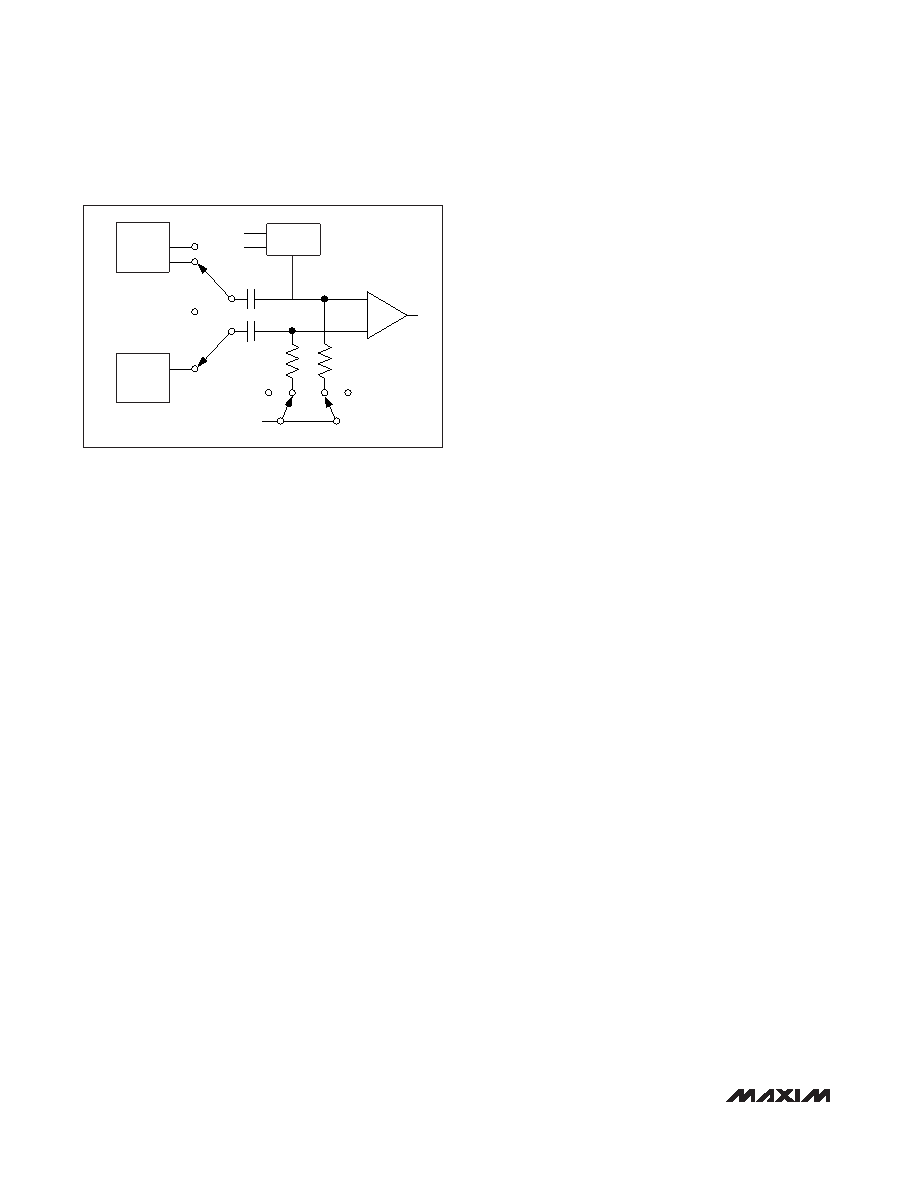
RIN+
+
-
HOLD
RIN-
CIN+
REF
GND
DAC
CIN-
TRACK
VDD/2
COMPARATOR
GND(AIN-)
AIN2
AIN1(AIN+)
HOLD
*( ) APPLIES TO MAX1088/1089
Figure 4. Equivalent Input Circuit
相关PDF资料 |
PDF描述 |
|---|---|
| VI-B54-IV-F2 | CONVERTER MOD DC/DC 48V 150W |
| VI-2TP-IW-F3 | CONVERTER MOD DC/DC 13.8V 100W |
| VE-BTJ-MX-F3 | CONVERTER MOD DC/DC 36V 75W |
| VI-2TP-IW-F2 | CONVERTER MOD DC/DC 13.8V 100W |
| D5FB | CONN RCPT FEMALE 5PIN BLK/SILVER |
相关代理商/技术参数 |
参数描述 |
|---|---|
| MAX1086EVKIT | 制造商:MAXIM 制造商全称:Maxim Integrated Products 功能描述:Evaluation Kit and Evaluation System for the MAX1286/MAX1288/MAX1086/MAX1088 |
| MAX1087 | 制造商:MAXIM 制造商全称:Maxim Integrated Products 功能描述:150ksps.10-Bit.2-Channel Single-Ended.and 1-Channel True-Differential ADCs in SOT23 |
| MAX1087EKA | 制造商:Maxim Integrated Products 功能描述:- Cut Tape Product |
| MAX1087EKA-T | 功能描述:模数转换器 - ADC RoHS:否 制造商:Texas Instruments 通道数量:2 结构:Sigma-Delta 转换速率:125 SPs to 8 KSPs 分辨率:24 bit 输入类型:Differential 信噪比:107 dB 接口类型:SPI 工作电源电压:1.7 V to 3.6 V, 2.7 V to 5.25 V 最大工作温度:+ 85 C 安装风格:SMD/SMT 封装 / 箱体:VQFN-32 |
| MAX1087ETA | 制造商:Rochester Electronics LLC 功能描述: 制造商:Maxim Integrated Products 功能描述: |
发布紧急采购,3分钟左右您将得到回复。