- 您现在的位置:买卖IC网 > PDF目录9921 > MAX1090BEEI+T (Maxim Integrated Products)IC ADC 10BIT 400KSPS 28-QSOP PDF资料下载
参数资料
| 型号: | MAX1090BEEI+T |
| 厂商: | Maxim Integrated Products |
| 文件页数: | 3/20页 |
| 文件大小: | 0K |
| 描述: | IC ADC 10BIT 400KSPS 28-QSOP |
| 产品培训模块: | Lead (SnPb) Finish for COTS Obsolescence Mitigation Program |
| 标准包装: | 2,500 |
| 位数: | 10 |
| 采样率(每秒): | 400k |
| 数据接口: | 并联 |
| 转换器数目: | 1 |
| 功率耗散(最大): | 667mW |
| 电压电源: | 单电源 |
| 工作温度: | -40°C ~ 85°C |
| 安装类型: | 表面贴装 |
| 封装/外壳: | 28-SSOP(0.154",3.90mm 宽) |
| 供应商设备封装: | 28-QSOP |
| 包装: | 带卷 (TR) |
| 输入数目和类型: | 8 个单端,单极;8 个单端,双极;4 个伪差分,单极;4 个伪差分,双极 |
MAX1090/MAX1092
400ksps, +5V, 8-/4-Channel, 10-Bit ADCs
with +2.5V Reference and Parallel Interface
______________________________________________________________________________________
11
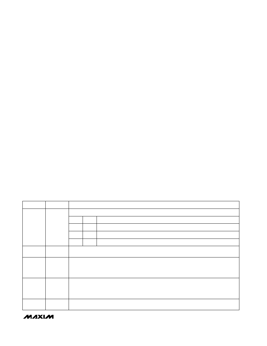
Table 1. Control Byte Functional Description
NAME
FUNCTION
D4
0
SGL/DIF
SGL/DIF = 0: Pseudo-Differential Analog Input Mode
SGL/DIF = 1: Single-Ended Analog Input Mode
In single-ended mode, input signals are referred to COM. In pseudo-differential mode, the voltage
difference between two channels is measured (Tables 2 and 3).
1
0
D3
UNI/BIP
Standby Power-Down Mode. Clock mode is unaffected.
0
1
UNI/BIP = 0: Bipolar Mode
UNI/BIP = 1: Unipolar Mode
In unipolar mode, an analog input signal from 0 to VREF can be converted; in bipolar mode, the
signal can range from -VREF/2 to +VREF/2.
D2, D1, D0
Normal Operation Mode. External clock mode is selected.
1
A2, A1, A0
Address bits A2, A1, A0 select which of the 8/4 (MAX1090/MAX1092) channels is to be converted
(Tables 3 and 4).
Normal Operation Mode. Internal clock mode is selected.
BIT
PD1, PD0
0
D7, D6
PD1 and PD0 select the various clock and power-down modes.
Full Power-Down Mode. Clock mode is unaffected.
D5
ACQMOD
ACQMOD = 0: Internal Acquisition Mode
ACQMOD = 1: External Acquisition Mode
initiate a combined acquisition plus conversion. The sam-
pling interval occurs at the end of the acquisition interval.
The ACQMOD (acquisition mode) bit in the input control
byte (Table 1) offers two options for acquiring the signal:
an internal and an external acquisition. The conversion
period lasts for 13 clock cycles in either the internal or
external clock or acquisition mode. Writing a new control
byte during a conversion cycle aborts the conversion and
starts a new acquisition interval.
Internal Acquisition
Select internal acquisition by writing the control byte
with the ACQMOD bit cleared (ACQMOD = 0). This
causes the write pulse to initiate an acquisition interval
whose duration is internally timed. Conversion starts
when this acquisition interval (three external clock
cycles or approximately 1s in internal clock mode)
ends (Figure 4). When the internal acquisition is com-
bined with the internal clock, the aperture jitter can be
as high as 200ps. Internal clock users wishing to
achieve the 50ps jitter specification should always use
external acquisition mode.
External Acquisition
Use external acquisition mode for precise control of the
sampling aperture and/or dependent control of acquisi-
tion and conversion times. The user controls acquisition
and start-of-conversion with two separate write pulses.
The first pulse, written with ACQMOD = 1, starts an
acquisition interval of indeterminate length. The second
write pulse, written with ACQMOD = 0 (all other bits in
the control byte are unchanged), terminates acquisition
and starts conversion on WR rising edge (Figure 5).
The address bits for the input multiplexer must have the
same values on the first and second write pulses.
Power-down mode bits (PD0, PD1) can assume new
values on the second write pulse (see the Power-Down
Modes section). Changing other bits in the control byte
corrupts the conversion.
Reading a Conversion
A standard interrupt signal, INT, is provided to allow the
MAX1090/MAX1092 to flag the P when the conversion
has ended and a valid result is available. INT goes low
when the conversion is complete and the output data is
ready (Figures 4 and 5). INT returns high on the first
read cycle or if a new control byte is written.
Selecting Clock Mode
The MAX1090/MAX1092 operate with an internal or
external clock. Control bits D6 and D7 select either
internal or external clock mode. The part retains the
last-requested clock mode if a power-down mode is
selected in the current input word. For both internal and
external clock modes, internal or external acquisition
can be used. At power-up, the MAX1090/MAX1092
enter the default external clock mode.
相关PDF资料 |
PDF描述 |
|---|---|
| MAX1091ACEI+T | IC ADC 10BIT 250KSPS 28-QSOP |
| MAX1091BEEI+T | IC ADC 10BIT 250KSPS 28-QSOP |
| MAX1142BCAP+T | IC ADC 14BIT 200KSPS 20-SSOP |
| MAX1143BCAP+T | IC ADC 14BIT 200KSPS 20-SSOP |
| MAX1145BCAP+T | IC ADC 14BIT 150KSPS 20-SSOP |
相关代理商/技术参数 |
参数描述 |
|---|---|
| MAX1091 | 制造商:MAXIM 制造商全称:Maxim Integrated Products 功能描述:250ksps, +3V, 8-/4-Channel, 10-Bit ADCs with +2.5V Reference and Parallel Interface |
| MAX1091ACEI | 功能描述:模数转换器 - ADC RoHS:否 制造商:Texas Instruments 通道数量:2 结构:Sigma-Delta 转换速率:125 SPs to 8 KSPs 分辨率:24 bit 输入类型:Differential 信噪比:107 dB 接口类型:SPI 工作电源电压:1.7 V to 3.6 V, 2.7 V to 5.25 V 最大工作温度:+ 85 C 安装风格:SMD/SMT 封装 / 箱体:VQFN-32 |
| MAX1091ACEI+ | 功能描述:模数转换器 - ADC 250ksps 8Ch 10-Bit w/Internal 2.5V ref RoHS:否 制造商:Texas Instruments 通道数量:2 结构:Sigma-Delta 转换速率:125 SPs to 8 KSPs 分辨率:24 bit 输入类型:Differential 信噪比:107 dB 接口类型:SPI 工作电源电压:1.7 V to 3.6 V, 2.7 V to 5.25 V 最大工作温度:+ 85 C 安装风格:SMD/SMT 封装 / 箱体:VQFN-32 |
| MAX1091ACEI+T | 功能描述:模数转换器 - ADC 250ksps 8Ch 10-Bit w/Internal 2.5V ref RoHS:否 制造商:Texas Instruments 通道数量:2 结构:Sigma-Delta 转换速率:125 SPs to 8 KSPs 分辨率:24 bit 输入类型:Differential 信噪比:107 dB 接口类型:SPI 工作电源电压:1.7 V to 3.6 V, 2.7 V to 5.25 V 最大工作温度:+ 85 C 安装风格:SMD/SMT 封装 / 箱体:VQFN-32 |
| MAX1091ACEI-T | 功能描述:模数转换器 - ADC RoHS:否 制造商:Texas Instruments 通道数量:2 结构:Sigma-Delta 转换速率:125 SPs to 8 KSPs 分辨率:24 bit 输入类型:Differential 信噪比:107 dB 接口类型:SPI 工作电源电压:1.7 V to 3.6 V, 2.7 V to 5.25 V 最大工作温度:+ 85 C 安装风格:SMD/SMT 封装 / 箱体:VQFN-32 |
发布紧急采购,3分钟左右您将得到回复。