- 您现在的位置:买卖IC网 > PDF目录9907 > MAX1092BCEG+ (Maxim Integrated Products)IC ADC 10BIT 400KSPS 24-QSOP PDF资料下载
参数资料
| 型号: | MAX1092BCEG+ |
| 厂商: | Maxim Integrated Products |
| 文件页数: | 7/20页 |
| 文件大小: | 0K |
| 描述: | IC ADC 10BIT 400KSPS 24-QSOP |
| 产品培训模块: | Lead (SnPb) Finish for COTS Obsolescence Mitigation Program |
| 标准包装: | 50 |
| 位数: | 10 |
| 采样率(每秒): | 400k |
| 数据接口: | 并联 |
| 转换器数目: | 1 |
| 功率耗散(最大): | 762mW |
| 电压电源: | 单电源 |
| 工作温度: | 0°C ~ 70°C |
| 安装类型: | 表面贴装 |
| 封装/外壳: | 24-SSOP(0.154",3.90mm 宽) |
| 供应商设备封装: | 24-QSOP |
| 包装: | 管件 |
| 输入数目和类型: | 4 个单端,单极;4 个单端,双极;2 个伪差分,单极;2 个伪差分,双极 |
___________Applications Information
Power-On Reset
When power is first applied, internal power-on reset cir-
cuitry activates the MAX1090/MAX1092 in external
clock mode and sets INT high. After the power supplies
stabilize, the internal reset time is 10s, and no conver-
sions should be attempted during this phase. When
using the internal reference, 500s are required for
VREF to stabilize.
Internal and External Reference
The MAX1090/MAX1092 can be used with an internal
or external reference voltage. An external reference
can be connected directly to REF or REFADJ.
An internal buffer is designed to provide +2.5V at REF
for both devices. The internally trimmed +1.22V refer-
ence is buffered with a +2.05V/V gain.
Internal Reference
The full-scale range with the internal reference is +2.5V
with unipolar inputs and ±1.25V with bipolar inputs. The
internal reference buffer allows for small adjustments
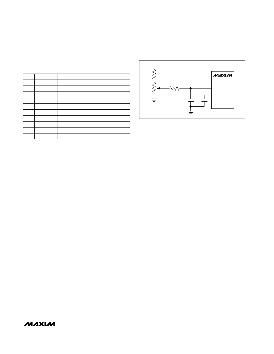
(±100mV) in the reference voltage (Figure 7).
Note: The reference buffer must be compensated with an
external capacitor (4.7F min) connected between REF
and GND to reduce reference noise and switching spikes
from the ADC. To further minimize reference noise, con-
nect a 0.01F capacitor between REFADJ and GND.
External Reference
With the MAX1090/MAX1092, an external reference can
be placed at either the input (REFADJ) or the output
(REF) of the internal reference-buffer amplifier.
Using the REFADJ input makes buffering the external
reference unnecessary. The REFADJ input impedance
is typically 17k
.
When applying an external reference to REF, disable
the internal reference buffer by connecting REFADJ to
VDD. The DC input resistance at REF is 25k
.
Therefore, an external reference at REF must deliver up
to 200A DC load current during a conversion and
have an output impedance less than 10
. If the refer-
ence has higher output impedance or is noisy, bypass
it close to the REF pin with a 4.7F capacitor.
Power-Down Modes
To save power, place the converter in a low-current
shutdown state between conversions. Select standby
mode or shutdown mode using bits D6 and D7 of the
control byte (Tables 1 and 2). In both software power-
down modes, the parallel interface remains active, but
the ADC does not convert.
Standby Mode
While in standby mode, the supply current is 1mA (typ).
The part powers up on the next rising edge on WR and
is ready to perform conversions. This quick turn-on time
allows the user to realize significantly reduced power
consumption for conversion rates below 400ksps.
Shutdown Mode
Shutdown mode turns off all chip functions that draw
quiescent current, reducing the typical supply current
to 2A immediately after the current conversion is com-
pleted. A rising edge on WR causes the MAX1090/
MAX1092 to exit shutdown mode and return to normal
operation. To achieve full 10-bit accuracy with a 4.7F
reference bypass capacitor, 500s is required after
power-up. Waiting 500s in standby mode, instead of in
full-power mode, can reduce power consumption by a
factor of 3 or more. When using an external reference,
MAX1090/MAX1092
400ksps, +5V, 8-/4-Channel, 10-Bit ADCs
with +2.5V Reference and Parallel Interface
______________________________________________________________________________________
15
Table 5. Data-Bus Output (8 + 2 Parallel
Interface)
VDD = +5V
330k
50k
GND
50k
0.01
F
4.7
F
REFADJ
REF
MAX1090
MAX1092
Figure 7. Reference Voltage Adjustment with External
Potentiometer
PIN
HBEN = 0
HBEN = 1
D0
Bit 0 (LSB)
Bit 8
D1
Bit 1
Bit 9 (MSB)
BIPOLAR
(UNI/BIP = 0)
UNIPOLAR
(UNI/BIP = 1)
D2
Bit 2
Bit 9
0
D5
Bit 5
Bit 9
0
D6
Bit 6
Bit 9
0
D7
Bit 7
Bit 9
0
D4
Bit 4
Bit 9
0
D3
Bit 3
Bit 9
0
相关PDF资料 |
PDF描述 |
|---|---|
| V48A12T500BL2 | CONVERTER MOD DC/DC 12V 500W |
| MAX1093BCEG+ | IC ADC 10BIT 250KSPS 24-QSOP |
| IDT72T3685L5BB | IC FIFO 16384X36 5NS 208-BGA |
| V48A12T500BL | CONVERTER MOD DC/DC 12V 500W |
| IDT72T1885L5BB | IC FIFO 32768X18 2.5V 5NS 144BGA |
相关代理商/技术参数 |
参数描述 |
|---|---|
| MAX1092BCEG+ | 功能描述:模数转换器 - ADC 400ksps 4Ch 10-Bit w/Internal 2.5V ref RoHS:否 制造商:Texas Instruments 通道数量:2 结构:Sigma-Delta 转换速率:125 SPs to 8 KSPs 分辨率:24 bit 输入类型:Differential 信噪比:107 dB 接口类型:SPI 工作电源电压:1.7 V to 3.6 V, 2.7 V to 5.25 V 最大工作温度:+ 85 C 安装风格:SMD/SMT 封装 / 箱体:VQFN-32 |
| MAX1092BCEG+T | 功能描述:模数转换器 - ADC 400ksps 4Ch 10-Bit w/Internal 2.5V ref RoHS:否 制造商:Texas Instruments 通道数量:2 结构:Sigma-Delta 转换速率:125 SPs to 8 KSPs 分辨率:24 bit 输入类型:Differential 信噪比:107 dB 接口类型:SPI 工作电源电压:1.7 V to 3.6 V, 2.7 V to 5.25 V 最大工作温度:+ 85 C 安装风格:SMD/SMT 封装 / 箱体:VQFN-32 |
| MAX1092BCEG-T | 功能描述:模数转换器 - ADC RoHS:否 制造商:Texas Instruments 通道数量:2 结构:Sigma-Delta 转换速率:125 SPs to 8 KSPs 分辨率:24 bit 输入类型:Differential 信噪比:107 dB 接口类型:SPI 工作电源电压:1.7 V to 3.6 V, 2.7 V to 5.25 V 最大工作温度:+ 85 C 安装风格:SMD/SMT 封装 / 箱体:VQFN-32 |
| MAX1092BCEI | 制造商:MAXIM 制造商全称:Maxim Integrated Products 功能描述:Analog to Digital Converter |
| MAX1092BEEG | 功能描述:模数转换器 - ADC RoHS:否 制造商:Texas Instruments 通道数量:2 结构:Sigma-Delta 转换速率:125 SPs to 8 KSPs 分辨率:24 bit 输入类型:Differential 信噪比:107 dB 接口类型:SPI 工作电源电压:1.7 V to 3.6 V, 2.7 V to 5.25 V 最大工作温度:+ 85 C 安装风格:SMD/SMT 封装 / 箱体:VQFN-32 |
发布紧急采购,3分钟左右您将得到回复。