- 您现在的位置:买卖IC网 > PDF目录10492 > MAX11040KGUU+ (Maxim Integrated Products)IC ADC 24BIT 4CH 38-TSSOP PDF资料下载
参数资料
| 型号: | MAX11040KGUU+ |
| 厂商: | Maxim Integrated Products |
| 文件页数: | 6/35页 |
| 文件大小: | 0K |
| 描述: | IC ADC 24BIT 4CH 38-TSSOP |
| 产品培训模块: | Lead (SnPb) Finish for COTS Obsolescence Mitigation Program |
| 标准包装: | 1 |
| 位数: | 24 |
| 采样率(每秒): | 3.07M |
| 数据接口: | DSP,MICROWIRE?,QSPI?,串行,SPI? |
| 转换器数目: | 4 |
| 功率耗散(最大): | 1.1W |
| 电压电源: | 模拟和数字 |
| 工作温度: | -40°C ~ 105°C |
| 安装类型: | 表面贴装 |
| 封装/外壳: | 38-TFSOP(0.173",4.40mm 宽) |
| 供应商设备封装: | 38-TSSOP |
| 包装: | 管件 |
| 输入数目和类型: | 4 个差分,双极 |
第1页第2页第3页第4页第5页当前第6页第7页第8页第9页第10页第11页第12页第13页第14页第15页第16页第17页第18页第19页第20页第21页第22页第23页第24页第25页第26页第27页第28页第29页第30页第31页第32页第33页第34页第35页
MAX11040K/MAX11060
24-/16-Bit, 4-Channel, Simultaneous-Sampling,
Cascadable, Sigma-Delta ADCs
14
Maxim Integrated
Modulator Clock
The modulator clock is created by dividing the frequen-
cy at the XIN input by a factor of 8. The XIN input is dri-
ven either directly by an external clock or by the
on-chip crystal oscillator.
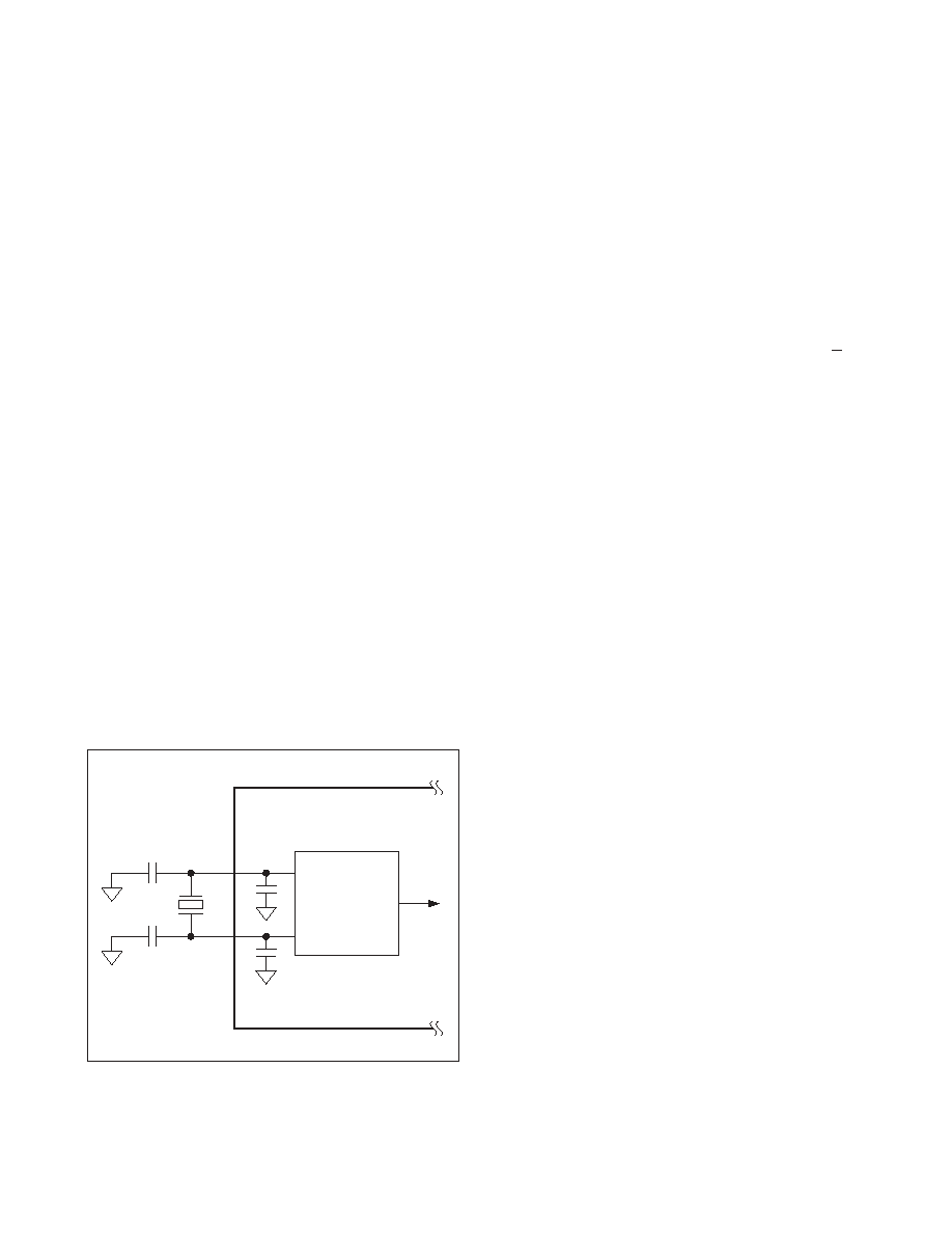
Crystal Oscillator
The on-chip oscillator requires an external crystal (or
resonator) with a 24.576MHz operating frequency con-
nected between XIN and XOUT, as shown in Figure 3.
As in any crystal-based oscillator circuit, the oscillator
frequency is sensitive to the capacitive load (CL). CL is
the capacitance that the crystal needs from the oscilla-
tor circuit and not the capacitance of the crystal. The
input capacitance across XIN and XOUT is 1.5pF.
Choose a crystal with a 24.576MHz oscillation frequen-
cy and an ESR less than 30
Ω, such as the MP35 from
RXD Technologies. See Figure 3 for the block diagram
of the crystal oscillator. Set XTALEN = 1 in the configu-
ration register to enable the crystal oscillator. The
CLKOUT output provides a buffered version of the
clock that is capable of driving eight devices, allowing
synchronized operation from a single crystal. See the
Multiple Device Synchronization section in the
Applications Information section.
External Clock
To use an external clock, set XTALEN = 0 in the
Configuration register and connect an external clock
source (20MHz–25MHz) to XIN. CLKOUT becomes
high impedance.
Analog Input Overvoltage
and Fault Protection
The full-scale differential input range of the devices is
±0.88VREF. The converter accurately represents any
input for which the positive and negative analog inputs
are separated by a magnitude of less than 0.88VREF.
The device includes special circuitry that protects it
against voltages on the analog inputs up to +6V.
Setting FAULTDIS = 1 disables the protection circuitry.
There are two mechanisms of overvoltage detection
and protection: full-scale overflow and overvoltage
fault. Full-scale overflow occurs if the magnitude of the
applied input voltage on any one or more channels is
greater than 0.88VREF. In this case, the digital output is
clipped to positive or negative full scale and the OVRFLW
flag goes low. Overvoltage fault occurs if the magni-
tude of an applied input voltage on any one or more
channels goes outside the fault-detection thresholds.
The reaction to an overvoltage fault is dependent on
whether the fault-protection circuitry is enabled. If
enabled, the input-protection circuits engage and the
FAULT flag goes low. A full-scale overflow or an over-
voltage fault condition on any one channel does not
affect the output data for the other channels.
The input protection circuits allow up to ±6V relative to
AGND on each input, and up to ±6V differentially
between AIN+ and AIN-, without damaging the devices
only if the following conditions are satisfied: power is
applied, the devices are not in shutdown mode, a clock
frequency of at least 20MHz is available at XIN, and
FAULTDIS = 0. The analog inputs allow up to ±3.5V rel-
ative to AGND when either devices are placed in shut-
down mode, the clock stops, or FAULTDIS = 1.
During an overvoltage fault condition, the impedance
between AIN_+ and AIN_- reduces to as low as 0.5k
Ω.
The output structure and cascading features of FAULT
and OVRFLW are discussed in the
Multiple Device
Digital Interface section.
Analog Input Overflow
Detection and Recovery (OVRFLW)
The OVRFLW flag is set based on the ADC conversion
result. When the applied voltage on one or more analog
inputs goes outside the positive or negative full scale
(±0.88VREF), OVRFLW asserts after a delay defined by
the latency of the converter, coincident with the DRDYOUT
of the full-scale clamped conversion result (see Figure
4). The specifics of the latency are discussed earlier in
the data sheet in the
Latency section.
MAX11040K
MAX11060
24.576MHz
20pF
XIN
XOUT
24.576MHz
OSCILLATOR
Figure 3. Crystal Oscillator Input
相关PDF资料 |
PDF描述 |
|---|---|
| UP050SL100J-A-B | CAP CER 10PF 50V 5% AXIAL |
| ICL7109CMH+D | IC ADC 12BIT 3-ST 44-MQFP |
| DS26303LN-120+ | IC LIU E1/T1/J1 3.3V 144-ELQFP |
| MS3116P10-98S | CONN PLUG 6POS STRAIGHT W/SCKT |
| MAX132CNG+ | IC ADC 18BIT W/SRL INTRFC 24-DIP |
相关代理商/技术参数 |
参数描述 |
|---|---|
| MAX11040KGUU/GG8 | 制造商:Maxim Integrated Products 功能描述:24-BIT, 4-CHANNEL, SIMULTANEOUS-SAMPLING, CASCADABLE, SIGMA- - Rail/Tube |
| MAX11040KGUU/GH9 | 制造商:Maxim Integrated Products 功能描述:24-BIT, 4-CHANNEL, SIMULTANEOUS-SAMPLING, CASCADABLE, SIGMA- - Rail/Tube |
| MAX11040KGUU+ | 功能描述:模数转换器 - ADC 24Bit 4Ch Simul-Samp Cascadable Sig Delt RoHS:否 制造商:Texas Instruments 通道数量:2 结构:Sigma-Delta 转换速率:125 SPs to 8 KSPs 分辨率:24 bit 输入类型:Differential 信噪比:107 dB 接口类型:SPI 工作电源电压:1.7 V to 3.6 V, 2.7 V to 5.25 V 最大工作温度:+ 85 C 安装风格:SMD/SMT 封装 / 箱体:VQFN-32 |
| MAX11040KGUU+T | 功能描述:模数转换器 - ADC 24Bit 4Ch Simul-Samp Cascadable Sig Delt RoHS:否 制造商:Texas Instruments 通道数量:2 结构:Sigma-Delta 转换速率:125 SPs to 8 KSPs 分辨率:24 bit 输入类型:Differential 信噪比:107 dB 接口类型:SPI 工作电源电压:1.7 V to 3.6 V, 2.7 V to 5.25 V 最大工作温度:+ 85 C 安装风格:SMD/SMT 封装 / 箱体:VQFN-32 |
| MAX11041 | 制造商:MAXIM 制造商全称:Maxim Integrated Products 功能描述:Wired Remote Controllers |
发布紧急采购,3分钟左右您将得到回复。