- 您现在的位置:买卖IC网 > PDF目录1935 > MAX11043ATL+T (Maxim Integrated Products)IC ADC 16BIT W/DAC 40-TQFN-EP PDF资料下载
参数资料
| 型号: | MAX11043ATL+T |
| 厂商: | Maxim Integrated Products |
| 文件页数: | 12/33页 |
| 文件大小: | 0K |
| 描述: | IC ADC 16BIT W/DAC 40-TQFN-EP |
| 产品培训模块: | Lead (SnPb) Finish for COTS Obsolescence Mitigation Program |
| 标准包装: | 2,500 |
| 类型: | ADC,DAC |
| 分辨率(位): | 16 b |
| 采样率(每秒): | 9.6M |
| 数据接口: | 串行 |
| 电压电源: | 模拟和数字 |
| 电源电压: | 3 V ~ 3.6 V |
| 工作温度: | -40°C ~ 125°C |
| 安装类型: | 表面贴装 |
| 封装/外壳: | 40-WFQFN 裸露焊盘 |
| 供应商设备封装: | 40-TQFN-EP(6x6) |
| 包装: | 带卷 (TR) |
第1页第2页第3页第4页第5页第6页第7页第8页第9页第10页第11页当前第12页第13页第14页第15页第16页第17页第18页第19页第20页第21页第22页第23页第24页第25页第26页第27页第28页第29页第30页第31页第32页第33页
MAX11043
4-Channel, 16-Bit, Simultaneous-Sampling ADCs
with PGA, Filter, and 8-/12-Bit Dual-Stage DAC
2
Maxim Integrated
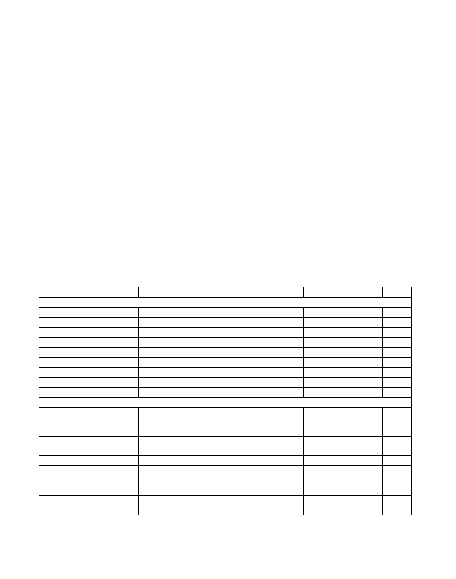
ABSOLUTE MAXIMUM RATINGS
ELECTRICAL CHARACTERISTICS
(VAVDD = +3.0V to +3.6V, VDVDD = +3.0V, CDVREG = 10F, VAGND = VDGND = 0V, common-mode input voltage = VAVDD/2, VREFBP
= VREFA = VREFB = VREFC = VREFD = +2.5V (external reference), VREFDAC = VREFDACH = +1.25V (external reference), VREFDACL =
0V, CREFBP = CREFA = CREFB = CREFC = CREFD = CREFDAC = 1F, fSCLK = 38.4MHz, fEXCLK = 38.4MHz (external clock applied to
OSCIN), clock divider set to 4, SHDN = DACSTEP = UP/DWN = DGND, CONVRUN = DVDD, all analog inputs driven directly through
a series 150
/330pF anti-alias filter, PGA gain = 1. Default filters and gain settings. DIFF = 1. TA = TMIN to TMAX, unless otherwise noted
(Note 1). Typical values are at TA = +25°C.)
Stresses beyond those listed under “Absolute Maximum Ratings” may cause permanent damage to the device. These are stress ratings only, and functional
operation of the device at these or any other conditions beyond those indicated in the operational sections of the specifications is not implied. Exposure to
absolute maximum rating conditions for extended periods may affect device reliability.
AVDD to AGND ....................................................-0.3V to +4.0V
DVDD to DGND .....................................................-0.3V to +4.0V
DVREG to DGND...................................................-0.3V to +3.0V
AGND to DGND.....................................................-0.3V to +0.3V
Analog I/O, REFDACH, REFDACL, REFA, REFB, REFC, REFD,
AOUT, REFDAC, REFBP to AGND .....-0.3V to (VAVDD + 0.3V)
UP/DWN, CONVRUN, SHDN, DACSTEP, EOC, Digital I/O,
OSCIN, OSCOUT to DGND....................-0.3V to (VDVDD + 0.3V)
Maximum Current into Any Pin except AVDD, DVDD, DVREG,
AGND, DGND...............................................................±50mA
Continuous Power Dissipation (TA = +70°C)
TQFN Multilayer Board
(derate 37mW/°C above +70°C) ................................2963mW
TQFN Single-Layer Board
(derate 26.3mW/°C above +70°C) ..........................2105.3mW
Operating Temperature Range .........................-40°C to +125°C
Junction Temperature ......................................................+150°C
Storage Temperature Range ............................-65°C to +150°C
Lead Temperature (soldering, 10s) ................................+300°C
Soldering Temperature (reflow) ......................................+260°C
PARAMETER
SYMBOL
CONDITIONS
MIN
TYP
MAX
UNITS
SIGMA-DELTA ADC
Resolution
N
16
Bits
Integral Nonlinearity
INL
-16
±2
LSB
Differential Nonlinearity
DNL
Guaranteed monotonic
-1
+1
LSB
Offset Error
OE
-35
+35
mV
Offset-Error Drift
±30
V/°C
Gain Error
GE
Trimmed with 150
/330pF anti-alias filter
-1
+1
%
Gain Temperature Coefficient
±50
ppm/°C
Channel Gain-Error Matching
Complete analog signal path
-0.25
+0.25
%
Channel Offset Matching
Complete analog signal path
-60
+60
mV
DYNAMIC PERFORMANCE (PGA Disabled, PGA Gain = 1 x (25kHz -1dB Full-Scale Signal))
Maximum Full-Scale Input
ADC modulator gain = 1
1.2
VP-P
Input-Referred Noise Spectral
Density
100kHz
85
nV/√Hz
Second Harmonic to
Fundamental
-80
-93
dB
Third Harmonic to Fundamental
-80
-110
dB
Spurious-Free Dynamic Range
SFDR
77
93
dB
Channel-to-Channel Isolation
Unused channels are shorted and
unconnected
85
108
dB
Channel Phase Matching
Between all channels, including complete
analog signal path
-0.05
+0.05
Degrees
相关PDF资料 |
PDF描述 |
|---|---|
| MAX11359AETL+T | IC DAS SYSTEM 16BIT 40-TQFN |
| MAX115CAX+ | IC DAS SYSTEM 12BIT 36-SSOP |
| MAX1221BETX+T | IC ADC/DAC 12BIT W/FIFO 36TQFNEP |
| MAX1257BETM+T | IC ADC/DAC 12BIT 48-TQFN |
| MAX125CCAX+D | IC DAS 14BIT 2X4CH 36-SSOP |
相关代理商/技术参数 |
参数描述 |
|---|---|
| MAX11044 | 制造商:MAXIM 制造商全称:Maxim Integrated Products 功能描述:4-/6-/8-Channel, 16-Bit, Simultaneous-Sampling ADCs |
| MAX11044_10 | 制造商:MAXIM 制造商全称:Maxim Integrated Products 功能描述:4-/6-/8-Channel, 16-Bit, Simultaneous-Sampling ADCs |
| MAX11044_11 | 制造商:MAXIM 制造商全称:Maxim Integrated Products 功能描述:4-/6-/8-Channel, 16-/14-Bit, Simultaneous-Sampling ADCs |
| MAX11044_12 | 制造商:MAXIM 制造商全称:Maxim Integrated Products 功能描述:4-/6-/8-Channel, 16-/14-Bit, Simultaneous-Sampling ADCs |
| MAX11044BECB+ | 功能描述:模数转换器 - ADC MAX11044BECB+ RoHS:否 制造商:Maxim Integrated 通道数量: 结构: 转换速率: 分辨率: 输入类型: 信噪比: 接口类型: 工作电源电压: 最大工作温度: 安装风格: 封装 / 箱体: |
发布紧急采购,3分钟左右您将得到回复。