- 您现在的位置:买卖IC网 > PDF目录2085 > MAX1108EUB+TG07 (Maxim Integrated Products)IC ADC 8BIT SPI/SRL 50K 10UMAX PDF资料下载
参数资料
| 型号: | MAX1108EUB+TG07 |
| 厂商: | Maxim Integrated Products |
| 文件页数: | 9/20页 |
| 文件大小: | 0K |
| 描述: | IC ADC 8BIT SPI/SRL 50K 10UMAX |
| 产品培训模块: | Lead (SnPb) Finish for COTS Obsolescence Mitigation Program |
| 标准包装: | 2,500 |
| 位数: | 8 |
| 采样率(每秒): | 50k |
| 数据接口: | MICROWIRE?,QSPI?,串行,SPI? |
| 转换器数目: | 1 |
| 功率耗散(最大): | 444mW |
| 电压电源: | 单电源 |
| 工作温度: | -40°C ~ 85°C |
| 安装类型: | 表面贴装 |
| 封装/外壳: | 10-TFSOP,10-MSOP(0.118",3.00mm 宽) |
| 供应商设备封装: | 10-µMAX |
| 包装: | 带卷 (TR) |
| 输入数目和类型: | 2 个单端,单极;2 个单端,双极;1 个伪差分,单极;1 个伪差分,双极 |
In external clock mode, if CS is toggled before the cur-
rent conversion is complete, the current conversion is
terminated, and the next high bit clocked into DIN is
recognized as a new start bit. This can be useful in
extending acquisition time by selecting conversion on
the same channel with the second control byte (double-
clocking mode), effectively extending acquisition to 6
SCLKs. This technique is ideal if the analog input
source has high impedance, or if it requires more than
1s to settle; it can also be used to allow the device
and the reference to settle when using power down-
modes (see Power-Down Modes section).
__________Applications Information
Battery Monitoring Mode
This mode of operation samples and converts the mid-
supply voltage, VDD / 2, which is internally generated.
Set SEL2 = SEL1 = SEL0 = 0 in the control byte to
select this configuration. This allows the user to monitor
the condition of a battery providing VDD. The reference
voltage must be larger than VDD / 2 for this mode of
operation to work properly. From the result of conver-
sion (CODE), VDD is determined as follows:
VDD = CODE VREF / 128.
Power-On Configuration
When power is first applied, the MAX1108/MAX1109’s
reference is powered down and SHDN is not enabled.
The device needs to be configured by setting CS low
and writing the control byte. Conversion can be started
within 20s if an external reference is used. When using
the internal reference, allow 12ms for the reference to
settle. This is done by first performing a configuration
conversion to power up the reference and then perform-
ing a second conversion once the reference is settled. No
conversions should be considered correct until the refer-
ence voltage (internal or external) has stabilized.
Power-Down Modes
To save power, place the converter into low-current
power-down mode between conversions. Minimum
power consumption is achieved by programming
REFSHDN = 0 and SHDN = 0 in the input control byte
(Table 4). When software power-down is asserted, it
becomes effective only after the conversion. If the con-
trol byte contains REFSHDN = 0, then the reference will
turn off at the end of conversion. If SHDN = 0, then the
chip will power-down at the end of conversion (in this
mode I/EREF or REFSHDN should also be set to zero).
Table 4 lists the power-down modes of the MAX1108/
MAX1109.
The first logical 1 clocked into DIN after CS falls powers
up the MAX1108/MAX1109 (20s required for the
device to power up). The reference is powered up only
if internal reference was selected during the previous
conversion. When the reference is powered up after
being disabled, consider the settling time before using
the result of conversion. Typically, 12ms are required
for the reference to settle from a discharge state; less
time may be considered if the external capacitor is not
discharged completely when exiting shutdown. In all
power-down modes, the interface remains active and
conversion results may be read. Use the double clock-
ing technique described in the Data Framing section to
allow more time for the reference to settle before start-
ing a conversion after short power-down.
Voltage Reference
The MAX1108/MAX1109 operate from a single supply
and feature a software-controlled internal reference of
+2.048V (MAX1108) and +4.096V (MAX1109). The
device can operate with either the internal reference or
an external reference applied at the REF pin. See the
Power-Down Modes and Modes of Operation sections
for detailed instructions on reference configuration.
The reference voltage determines the full-scale range:
in unipolar mode, the input range is from 0 to VREF; in
bipolar mode, the input range spans RI ±VREF / 2 with
RI = VREF / 2.
MAX1108/MAX1109
Single-Supply, Low-Power,
2-Channel, Serial 8-Bit ADCs
______________________________________________________________________________________
17
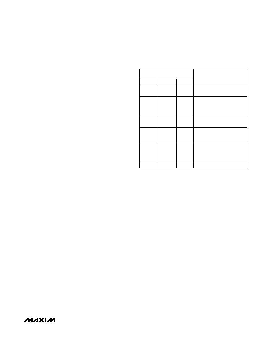
Table 4. Power-Down Modes of the
MAX1108/MAX1109
1
BIT 2–BIT 0 OF
CONTROL BYTE
1
0
1
0
1
X
1
0
1
0
X
REFSHDN
I/EREF
SHDN
OPERATING MODE
Device Active; Internal refer-
ence powered down after con-
version, powered up at next
start bit.
Device Active/Internal
Reference Active
Device and internal reference
powered down after conversion,
powered up at next start bit.
Device Active/External
Reference Mode
Reserved. Do not use.
Device powered down after
each conversion, powered up
at next start bit. External
Reference Mode.
X = Don’t care
相关PDF资料 |
PDF描述 |
|---|---|
| MAX110AEWE+ | IC ADC 14BIT 2CH 16-SOIC |
| MAX11131ATI+ | IC ADC 12BIT SRL 28-TQFN-EP |
| MAX1118EKA+T | IC ADC 8-BIT 100KSPS SOT23-8 |
| MAX11205BEUB+T | IC ADC 16BIT SRL 13.75SPS 10UMAX |
| MAX11206EEE+ | IC ADC 20BIT 16QSOP |
相关代理商/技术参数 |
参数描述 |
|---|---|
| MAX1108-MAX1109 | 制造商:MAXIM 制造商全称:Maxim Integrated Products 功能描述:Single-Supply, Low-Power, 2-Channel, Serial 8-Bit ADCs |
| MAX1109 | 制造商:MAXIM 制造商全称:Maxim Integrated Products 功能描述:Evaluation Kit for the MAX4135/MAX4136/MAX4137/MAX4138[MAX4135EVKIT ] |
| MAX1109CUB | 功能描述:模数转换器 - ADC RoHS:否 制造商:Texas Instruments 通道数量:2 结构:Sigma-Delta 转换速率:125 SPs to 8 KSPs 分辨率:24 bit 输入类型:Differential 信噪比:107 dB 接口类型:SPI 工作电源电压:1.7 V to 3.6 V, 2.7 V to 5.25 V 最大工作温度:+ 85 C 安装风格:SMD/SMT 封装 / 箱体:VQFN-32 |
| MAX1109CUB+ | 功能描述:模数转换器 - ADC 2Ch Single-Supply Low-P Serial 8-Bit RoHS:否 制造商:Texas Instruments 通道数量:2 结构:Sigma-Delta 转换速率:125 SPs to 8 KSPs 分辨率:24 bit 输入类型:Differential 信噪比:107 dB 接口类型:SPI 工作电源电压:1.7 V to 3.6 V, 2.7 V to 5.25 V 最大工作温度:+ 85 C 安装风格:SMD/SMT 封装 / 箱体:VQFN-32 |
| MAX1109CUB+G07 | 制造商:Maxim Integrated Products 功能描述:10 PINS UMAX PKG - Tape and Reel |
发布紧急采购,3分钟左右您将得到回复。