参数资料
| 型号: | MAX1111CPE+ |
| 厂商: | Maxim Integrated Products |
| 文件页数: | 19/20页 |
| 文件大小: | 0K |
| 描述: | IC ADC 8BIT LP 16-DIP |
| 标准包装: | 25 |
| 位数: | 8 |
| 采样率(每秒): | 50k |
| 数据接口: | MICROWIRE?,QSPI?,串行,SPI? |
| 转换器数目: | 1 |
| 功率耗散(最大): | 667mW |
| 电压电源: | 单电源 |
| 工作温度: | 0°C ~ 70°C |
| 安装类型: | 通孔 |
| 封装/外壳: | 16-DIP(0.300",7.62mm) |
| 供应商设备封装: | 16-PDIP |
| 包装: | 管件 |
| 输入数目和类型: | 4 个单端,单极;2 个差分,单极 |
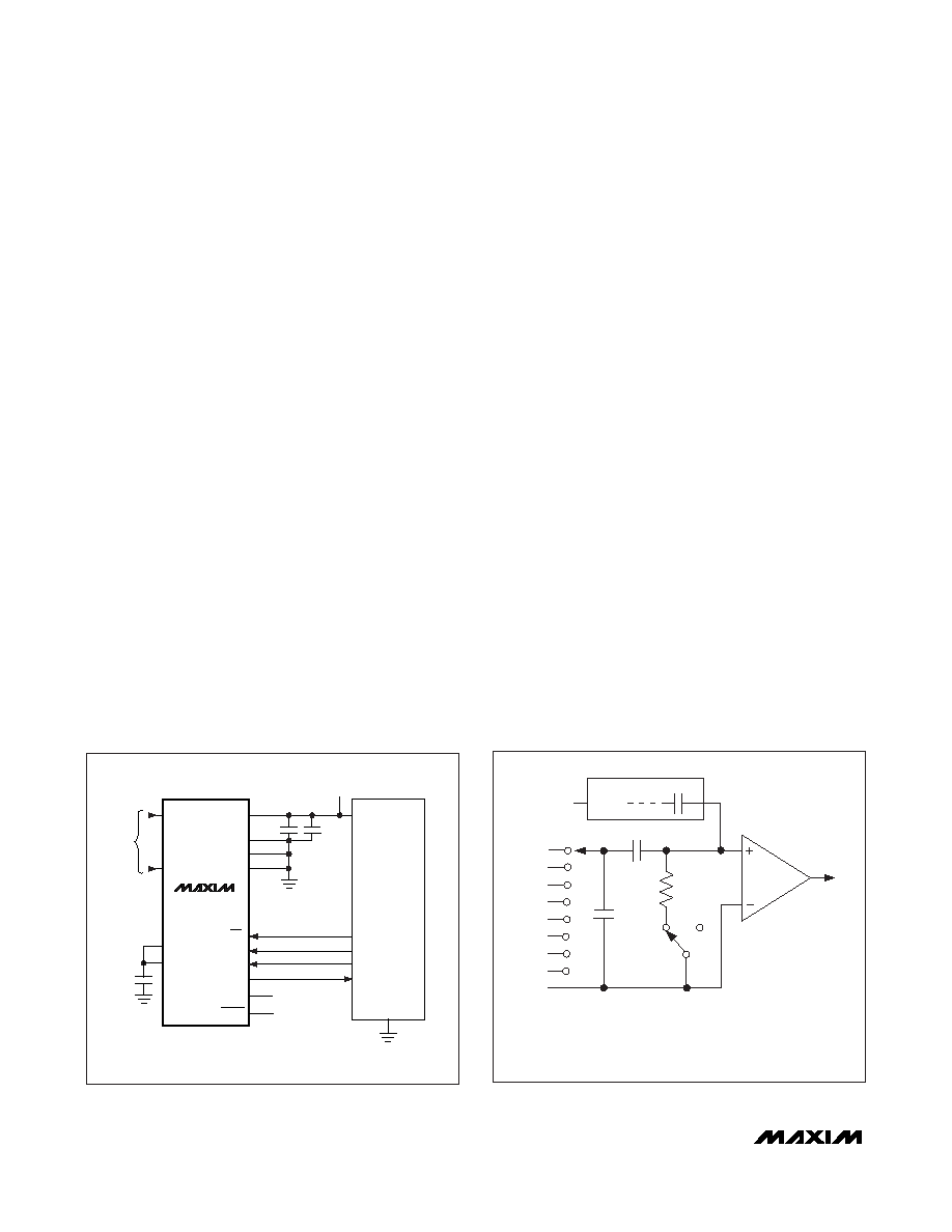
_______________Detailed Description
The MAX1110/MAX1111 analog-to-digital converters
(ADCs) use a successive-approximation conversion
technique and input track/hold (T/H) circuitry to convert
an analog signal to an 8-bit digital output. A flexible seri-
al interface provides easy interface to microprocessors
(Ps). Figure 3 shows the Typical Operating Circuit.
Pseudo-Differential Input
The sampling architecture of the ADC’s analog com-
parator is illustrated in Figure 4, the equivalent input cir-
cuit. In single-ended mode, IN+ is internally switched to
the selected input channel, CH_, and IN- is switched to
COM. In differential mode, IN+ and IN- are selected
from the following pairs: CH0/CH1, CH2/CH3,
CH4/CH5, and CH6/CH7. Configure the MAX1110
channels with Table 1 and the MAX1111 channels with
Table 2.
In differential mode, IN- and IN+ are internally switched
to either of the analog inputs. This configuration is
pseudo-differential to the effect that only the signal at
IN+ is sampled. The return side (IN-) must remain sta-
ble within ±0.5 LSB (±0.1 LSB for best results) with
respect to AGND during a conversion. To accomplish
this, connect a 0.1F capacitor from IN- (the selected
analog input) to AGND.
During the acquisition interval, the channel selected as
the positive input (IN+) charges capacitor CHOLD. The
acquisition interval spans two SCLK cycles and ends
on the falling SCLK edge after the last bit of the input
control word has been entered. At the end of the acqui-
sition interval, the T/H switch opens, retaining charge
on CHOLD as a sample of the signal at IN+. The conver-
sion interval begins with the input multiplexer switching
CHOLD from the positive input (IN+) to the negative
input (IN-). In single-ended mode, IN- is simply COM.
This unbalances node ZERO at the input of the com-
parator. The capacitive DAC adjusts during the remain-
der of the conversion cycle to restore node ZERO to 0V
within the limits of 8-bit resolution. This action is equiva-
lent to transferring a charge of 18pF x (VIN+ - VIN-) from
CHOLD to the binary-weighted capacitive DAC, which in
turn forms a digital representation of the analog input
signal.
Track/Hold
The T/H enters its tracking mode on the falling clock
edge after the sixth bit of the 8-bit control byte has
been shifted in. It enters its hold mode on the falling
clock edge after the eighth bit of the control byte has
been shifted in. If the converter is set up for single-
ended inputs, IN- is connected to COM, and the con-
verter samples the “+” input; if it is set up for differential
inputs, IN- connects to the “-” input, and the difference
(IN+ - IN-) is sampled. At the end of the conversion, the
positive input connects back to IN+, and CHOLD
charges to the input signal.
MAX1110/MAX1111
+2.7V, Low-Power, Multichannel,
Serial 8-Bit ADCs
8
_______________________________________________________________________________________
VDD
I/O
SCK (SK)
MOSI (SO)
MISO (SI)
VSS
SHDN
SSTRB
DOUT
DIN
SCLK
CS
COM
DGND
AGND
VDD
CH7
1
μF
0.1
μF
1
μF
CH0
ANALOG
INPUTS
MAX1110
MAX1111
CPU
+2.7V
REFIN
REFOUT
Figure 3. Typical Operating Circuit
CH0
CH1
CH2
CH3
CH4*
CH5*
CH6*
CH7*
COM
CSWITCH
TRACK
T/H
SWITCH
CHOLD
HOLD
CAPACITIVE DAC
REFIN
ZERO
COMPARATOR
–
+
18pF
6.5k
Ω
RIN
SINGLE-ENDED MODE: IN+ = CHO–CH7, IN- = COM.
DIFFERENTIAL MODE: IN+ AND IN- SELECTED FROM PAIRS OF
CH0/CH1, CH2/CH3, CH4*/CH5*, CH6*/CH7*.
*MAX1110 ONLY
AT THE SAMPLING INSTANT,
THE MUX INPUT SWITCHES
FROM THE SELECTED IN+
CHANNEL TO THE SELECTED
IN- CHANNEL.
INPUT
MUX
Figure 4. Equivalent Input Circuit
相关PDF资料 |
PDF描述 |
|---|---|
| MAX1113CPE+ | IC ADC 8BIT LP 16-DIP |
| MAX1116EKA+T | IC ADC 8BIT SERIAL SOT23-8 |
| MAX11201BEUB+T | IC ADC 24BIT SRL 13.75SPS 10UMAX |
| MAX11202BEUB+T | IC ADC 24BIT SRL 13.75SPS 10UMAX |
| MAX11210EEE+T | ADC 24BIT 4WIRE SPI 16-QSOP |
相关代理商/技术参数 |
参数描述 |
|---|---|
| MAX1111CPE+ | 功能描述:模数转换器 - ADC 2.7V Low-Power Multi Ch Serial 8-Bit RoHS:否 制造商:Texas Instruments 通道数量:2 结构:Sigma-Delta 转换速率:125 SPs to 8 KSPs 分辨率:24 bit 输入类型:Differential 信噪比:107 dB 接口类型:SPI 工作电源电压:1.7 V to 3.6 V, 2.7 V to 5.25 V 最大工作温度:+ 85 C 安装风格:SMD/SMT 封装 / 箱体:VQFN-32 |
| MAX1111EEE | 功能描述:模数转换器 - ADC RoHS:否 制造商:Texas Instruments 通道数量:2 结构:Sigma-Delta 转换速率:125 SPs to 8 KSPs 分辨率:24 bit 输入类型:Differential 信噪比:107 dB 接口类型:SPI 工作电源电压:1.7 V to 3.6 V, 2.7 V to 5.25 V 最大工作温度:+ 85 C 安装风格:SMD/SMT 封装 / 箱体:VQFN-32 |
| MAX1111EEE/V+ | 功能描述:模数转换器 - ADC 2.7V Low-Power Multi Ch Serial 8-Bit RoHS:否 制造商:Texas Instruments 通道数量:2 结构:Sigma-Delta 转换速率:125 SPs to 8 KSPs 分辨率:24 bit 输入类型:Differential 信噪比:107 dB 接口类型:SPI 工作电源电压:1.7 V to 3.6 V, 2.7 V to 5.25 V 最大工作温度:+ 85 C 安装风格:SMD/SMT 封装 / 箱体:VQFN-32 |
| MAX1111EEE/V+T | 功能描述:模数转换器 - ADC 2.7V Low-Power Multi Ch Serial 8-Bit RoHS:否 制造商:Texas Instruments 通道数量:2 结构:Sigma-Delta 转换速率:125 SPs to 8 KSPs 分辨率:24 bit 输入类型:Differential 信噪比:107 dB 接口类型:SPI 工作电源电压:1.7 V to 3.6 V, 2.7 V to 5.25 V 最大工作温度:+ 85 C 安装风格:SMD/SMT 封装 / 箱体:VQFN-32 |
| MAX1111EEE+ | 功能描述:模数转换器 - ADC 2.7V Low-Power Multi Ch Serial 8-Bit RoHS:否 制造商:Texas Instruments 通道数量:2 结构:Sigma-Delta 转换速率:125 SPs to 8 KSPs 分辨率:24 bit 输入类型:Differential 信噪比:107 dB 接口类型:SPI 工作电源电压:1.7 V to 3.6 V, 2.7 V to 5.25 V 最大工作温度:+ 85 C 安装风格:SMD/SMT 封装 / 箱体:VQFN-32 |
发布紧急采购,3分钟左右您将得到回复。