- 您现在的位置:买卖IC网 > PDF目录2008 > MAX1135BCAP+ (Maxim Integrated Products)IC ADC 16BIT 150KSPS 20-SSOP PDF资料下载
参数资料
| 型号: | MAX1135BCAP+ |
| 厂商: | Maxim Integrated Products |
| 文件页数: | 5/18页 |
| 文件大小: | 0K |
| 描述: | IC ADC 16BIT 150KSPS 20-SSOP |
| 产品培训模块: | Lead (SnPb) Finish for COTS Obsolescence Mitigation Program |
| 标准包装: | 66 |
| 位数: | 16 |
| 采样率(每秒): | 150k |
| 数据接口: | MICROWIRE?,QSPI?,串行,SPI? |
| 转换器数目: | 1 |
| 功率耗散(最大): | 26.4mW |
| 电压电源: | 模拟和数字 |
| 工作温度: | 0°C ~ 70°C |
| 安装类型: | 表面贴装 |
| 封装/外壳: | 20-SSOP(0.209",5.30mm 宽) |
| 供应商设备封装: | 20-SSOP |
| 包装: | 管件 |
| 输入数目和类型: | 1 个单端,单极;1 个单端,双极 |
Input Acquisition and Settling
Clocking in a control byte starts input acquisition. The
main capacitor array starts acquiring the input as soon
as a start bit is recognized, using the same input range
as the previous conversion. If the opposite input range
is selected by the second DIN bit, the part immediately
switches to the new sampling mode. Acquisition time is
one-and-a-half clock cycles shorter when switching
from unipolar to bipolar or bipolar to unipolar modes
than when continuously converting in the same mode.
Acquisition can be extended by eight clock cycles by
setting M1 = 1 and M0 = 1 (long acquisition mode). The
sampling instant in short acquisition completes on the
falling edge of the sixth clock cycle after the start bit
(Figure 2). Acquisition is five clock cycles in short
acquisition mode and 13 clock cycles in long acquisi-
tion mode. Short acquisition mode is 24 clock cycles
per conversion. Using the external clock to run the con-
version process limits unipolar conversion speed to
125ksps instead of 150ksps as in bipolar mode. The
input resistance in unipolar mode is larger than that of
bipolar mode (Figure 1). The RC time constant in unipo-
lar mode is larger than that of bipolar mode, reducing
the maximum conversion rate in 24 external clock
mode. Long acquisition mode with external clock
allows both unipolar and bipolar sampling of 112ksps
(3.6MHz / 32 clock cycles) by adding eight extra clock
cycles to the conversion.
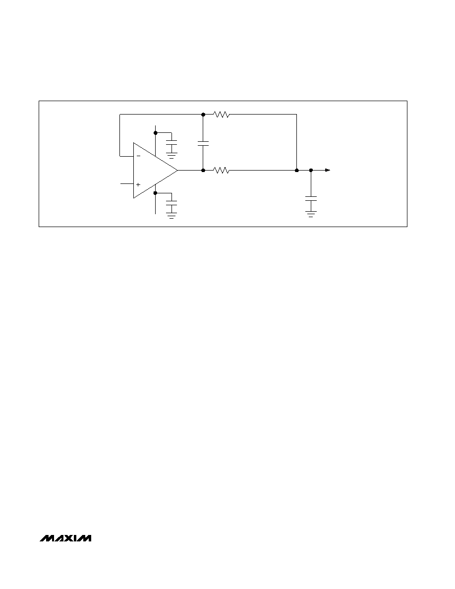
Most applications require an input buffer amplifier. If
the input signal is multiplexed, the input channel should
be switched immediately after acquisition, rather than
near the end of or after a conversion. This allows more
time for the input buffer amplifier to respond to a large
step change in input signal. The input amplifier must
have a high enough slew rate to complete the required
output voltage change before the beginning of the
acquisition time.
At the beginning of acquisition, the capacitive DAC is
connected to the amplifier output, causing some output
disturbance. Ensure that the sampled voltage has set-
tled to within the required limits before the end of the
acquisition time. If the frequency of interest is low, AIN
can be bypassed with a large enough capacitor to
charge the capacitive DAC with very little change in
voltage. However, for AC use, AIN must be driven by a
wideband buffer (at least 10MHz), which must be sta-
ble with the DAC’s capacitive load (in parallel with any
AIN bypass capacitor used) and also must settle quickly
(Figure 7).
Digital Noise
Digital noise can couple to AIN and REF. The conver-
sion clock (SCLK) and other digital signals that are
active during input acquisition contribute noise to the
conversion result. If the noise signal is synchronous to
the sampling interval, an effective input offset is pro-
duced.
Asynchronous signals produce random noise on the
input, whose high-frequency components may be
aliased into the frequency band of interest. Minimize
noise by presenting a low impedance (at the frequen-
cies contained in the noise signal) at the inputs. This
requires bypassing AIN to AGND, or buffering the input
with an amplifier that has a small-signal bandwidth of
several MHz, or preferably both. AIN has a bandwidth
of about 4MHz.
MAX1134/MAX1135
16-Bit ADCs, 150ksps, 3.3V Single Supply
______________________________________________________________________________________
13
4
7
6
2
3
IN
VCC
VEE
0.0033
mF
0.1
mF
0.1
mF
100pF
1k
W
1k
W
AIN
Figure 7. AIN Buffer for AC/DC Use
相关PDF资料 |
PDF描述 |
|---|---|
| MAX1138LEEE+T | IC ADC 10BIT SERIAL 16-QSOP |
| MAX1159AEUI+ | IC ADC 14BIT 135KSPS 28-TSSOP |
| MAX11602EEE+ | IC ADC SERIAL 8BIT 8CH 16-QSOP |
| MAX11610EEE+T | IC ADC SERIAL 10BIT 12CH 16-QSOP |
| MAX11616EEE+T | IC ADC SERIAL 12BIT 12CH 16-QSOP |
相关代理商/技术参数 |
参数描述 |
|---|---|
| MAX1135BCAP+ | 功能描述:模数转换器 - ADC 16-Bit 150ksps 3.3V Single Supply RoHS:否 制造商:Texas Instruments 通道数量:2 结构:Sigma-Delta 转换速率:125 SPs to 8 KSPs 分辨率:24 bit 输入类型:Differential 信噪比:107 dB 接口类型:SPI 工作电源电压:1.7 V to 3.6 V, 2.7 V to 5.25 V 最大工作温度:+ 85 C 安装风格:SMD/SMT 封装 / 箱体:VQFN-32 |
| MAX1135BCAP+T | 功能描述:模数转换器 - ADC 16-Bit 150ksps 3.3V Single Supply RoHS:否 制造商:Texas Instruments 通道数量:2 结构:Sigma-Delta 转换速率:125 SPs to 8 KSPs 分辨率:24 bit 输入类型:Differential 信噪比:107 dB 接口类型:SPI 工作电源电压:1.7 V to 3.6 V, 2.7 V to 5.25 V 最大工作温度:+ 85 C 安装风格:SMD/SMT 封装 / 箱体:VQFN-32 |
| MAX1135BCAP-T | 功能描述:模数转换器 - ADC RoHS:否 制造商:Texas Instruments 通道数量:2 结构:Sigma-Delta 转换速率:125 SPs to 8 KSPs 分辨率:24 bit 输入类型:Differential 信噪比:107 dB 接口类型:SPI 工作电源电压:1.7 V to 3.6 V, 2.7 V to 5.25 V 最大工作温度:+ 85 C 安装风格:SMD/SMT 封装 / 箱体:VQFN-32 |
| MAX1135BEAP | 功能描述:模数转换器 - ADC RoHS:否 制造商:Texas Instruments 通道数量:2 结构:Sigma-Delta 转换速率:125 SPs to 8 KSPs 分辨率:24 bit 输入类型:Differential 信噪比:107 dB 接口类型:SPI 工作电源电压:1.7 V to 3.6 V, 2.7 V to 5.25 V 最大工作温度:+ 85 C 安装风格:SMD/SMT 封装 / 箱体:VQFN-32 |
| MAX1135BEAP+ | 功能描述:模数转换器 - ADC 16-Bit 150ksps 3.3V Single Supply RoHS:否 制造商:Texas Instruments 通道数量:2 结构:Sigma-Delta 转换速率:125 SPs to 8 KSPs 分辨率:24 bit 输入类型:Differential 信噪比:107 dB 接口类型:SPI 工作电源电压:1.7 V to 3.6 V, 2.7 V to 5.25 V 最大工作温度:+ 85 C 安装风格:SMD/SMT 封装 / 箱体:VQFN-32 |
发布紧急采购,3分钟左右您将得到回复。