- 您现在的位置:买卖IC网 > PDF目录9922 > MAX1144BCAP+T (Maxim Integrated Products)IC ADC 14BIT 150KSPS 20-SSOP PDF资料下载
参数资料
| 型号: | MAX1144BCAP+T |
| 厂商: | Maxim Integrated Products |
| 文件页数: | 4/18页 |
| 文件大小: | 0K |
| 描述: | IC ADC 14BIT 150KSPS 20-SSOP |
| 产品培训模块: | Lead (SnPb) Finish for COTS Obsolescence Mitigation Program |
| 标准包装: | 2,000 |
| 位数: | 14 |
| 采样率(每秒): | 150k |
| 数据接口: | DSP,MICROWIRE?,QSPI?,串行,SPI? |
| 转换器数目: | 1 |
| 功率耗散(最大): | 26.4mW |
| 电压电源: | 模拟和数字 |
| 工作温度: | 0°C ~ 70°C |
| 安装类型: | 表面贴装 |
| 封装/外壳: | 20-SSOP(0.209",5.30mm 宽) |
| 供应商设备封装: | 20-SSOP |
| 包装: | 带卷 (TR) |
| 输入数目和类型: | 1 个单端,单极;1 个单端,双极 |
MAX1144/MAX1145
When internal clock mode is selected, SSTRB does not
go into a high-impedance state when CS goes high.
Figure 6 shows the SSTRB timing in internal clock
mode. In internal clock mode, data can be shifted into
the MAX1144/MAX1145 at clock rates up to 4MHz, pro-
vided the minimum acquisition time, tACQ, is kept
above 1.39s in bipolar mode and 1.67s in unipolar
mode. Data can be clocked out at 4MHz.
Output Data
The output data format is straight binary for unipolar
conversions and two’s complement in bipolar mode.
The MSB is shifted out of the MAX1144/MAX1145 first
in both modes.
Data Framing
The falling edge of CS does not start a conversion on the
MAX1144/MAX1145. The first logic high clocked into
DIN is interpreted as a start bit and defines the first bit of
the control byte. A conversion starts on the falling edge
of SCLK, after the seventh bit of the control byte (the P1
bit) is clocked into DIN. The start bit is defined as:
The first high bit clocked into DIN with CS low any-
time the converter is idle, e.g. after AVDD is
applied.
The first high bit clocked into DIN after CS is pulsed
high then low.
If a falling edge on CS forces a start bit before the con-
version or calibration is complete, then the current
operation terminates and a new one starts.
Applications Information
Power-On Reset
When power is first applied to the MAX1144/MAX1145,
or if RST is pulsed low, the internal calibration registers
are set to their default values. The user-programmable
registers (P0, P1, and P2) are low, and the device is
configured for bipolar mode with internal clocking.
Calibration
Periodically calibrate the MAX1144/MAX1145 to com-
pensate for temperature drift and other variations. After
any change in ambient temperature more than +10°C,
the device should be recalibrated. A 100mV change in
supply voltage or any change in the reference voltage
should be followed by a calibration. Calibration cor-
rects for errors in gain, offset, integral nonlinearity, and
differential nonlinearity.
The MAX1144/MAX1145 should be calibrated after
power-up or after the assertion of reset. Make sure the
power supplies and the reference voltage have fully
settled prior to initiating the calibration sequence.
Initiate calibration by setting M1 = 0 and M0 = 1 in the
control byte. In internal clock mode, SSTRB goes low at
the beginning of calibration and goes high to signal the
end of calibration, approximately 80,000 clock cycles
later. In external clock mode, SSTRB goes high at the
beginning of calibration and goes low to signal the end
of calibration. Calibration should be performed in the
same clock mode that is used for conversions.
Reference
The MAX1144/MAX1145 require an external reference.
The external reference must be bypassed with a 4.7F
capacitor. The input impedance at REF is a minimum of
16k
for DC currents. During conversion, an external
reference at REF must deliver up to 150A DC load
current and have an output impedance of 10
or less.
Analog Input
The MAX1144/MAX1145 use a capacitive DAC that
provides an inherent track/hold function. Drive AIN with
a source impedance less than 10
. Any signal condi-
tioning circuitry must settle with 14-bit accuracy in less
than 500ns. Limit the input bandwidth to less than half
the sampling frequency to eliminate aliasing. The
MAX1144/MAX1145 have a complex input impedance
that varies from unipolar to bipolar mode (Figure 1).
Input Range
The analog input range in unipolar mode is 0 to +6V for
the MAX1144, and 0 to +2.048V for the MAX1145. In
bipolar mode, the analog input can be -6V to +6V for
the MAX1144, or -2.048V to +2.048V for the MAX1145.
Unipolar or bipolar mode is programmed with the
UNI/BIP bit of the control byte. When using a reference
other than the suggested +2.048V, the full-scale input
range varies accordingly. The full-scale input range
depends on the voltage at REF and the sampling mode
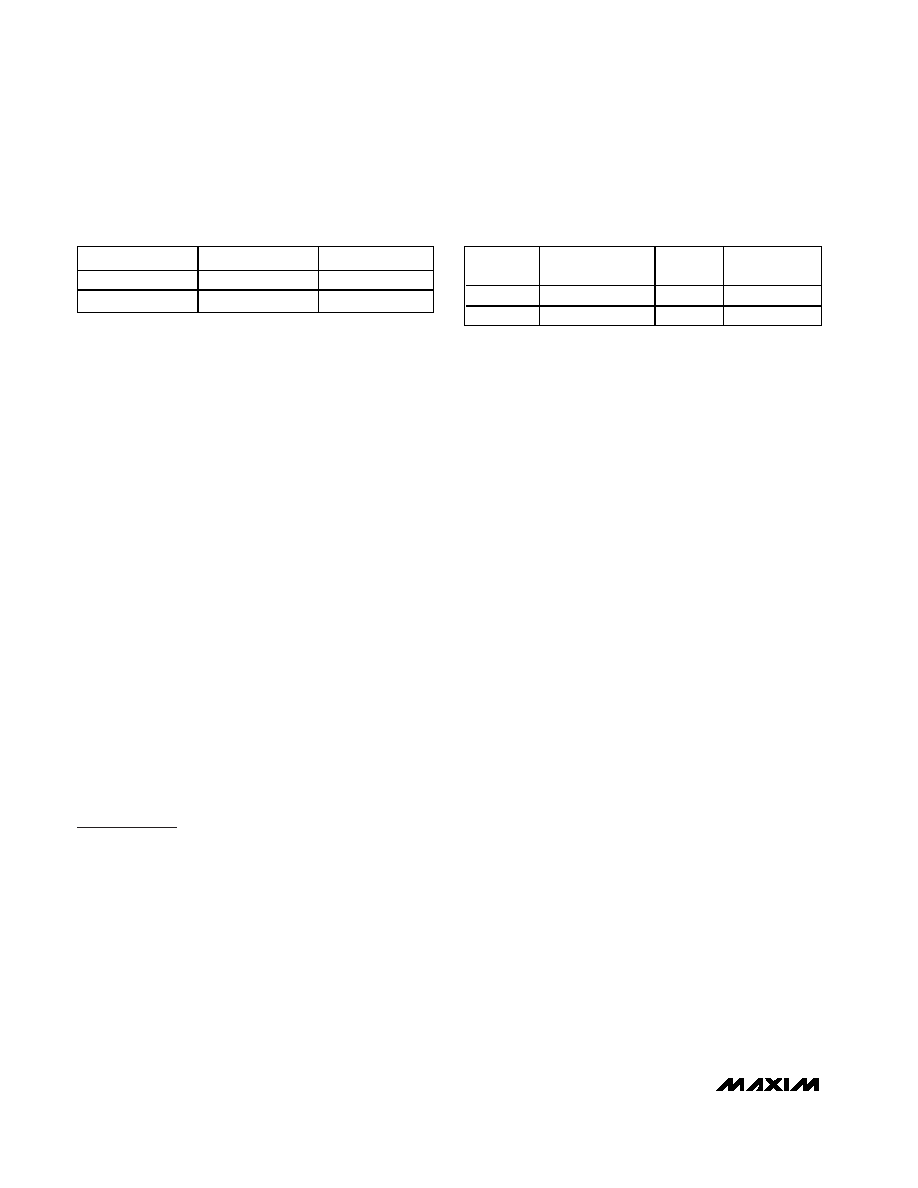
selected (Tables 3 and 4).
14-Bit ADCs, 150ksps, 3.3V Single Supply
12
______________________________________________________________________________________
PART
ZERO SCALE
FULL SCALE
MAX1144
0
6 (VREF/2.048)
MAX1145
0
VREF
PART
NEGATIVE FULL
SCALE
ZERO
SCALE
FULL SCALE
MAX1144
-6 (VREF/2.048)
0
+6 (VREF/2.048)
MAX1145
-VREF
0+VREF
Table 3. Unipolar Full Scale and Zero
Scale
Table 4. Bipolar Full Scale, Zero Scale,
and Negative Scale
相关PDF资料 |
PDF描述 |
|---|---|
| ICL3245ECBZ-T | IC 3DRVR/5RCVR RS232 3V 28-SOIC |
| ICL3245ECAZ-T | IC 3DRVR/5RCVR RS232 3V 28-SSOP |
| VE-24F-CU-B1 | CONVERTER MOD DC/DC 72V 200W |
| ISL32174EFVZ-T | IC XMITTER ESD RS422 LP 16-TSSOP |
| V300B24M250BG2 | CONVERTER MOD DC/DC 24V 250W |
相关代理商/技术参数 |
参数描述 |
|---|---|
| MAX1144BEAP | 功能描述:模数转换器 - ADC RoHS:否 制造商:Texas Instruments 通道数量:2 结构:Sigma-Delta 转换速率:125 SPs to 8 KSPs 分辨率:24 bit 输入类型:Differential 信噪比:107 dB 接口类型:SPI 工作电源电压:1.7 V to 3.6 V, 2.7 V to 5.25 V 最大工作温度:+ 85 C 安装风格:SMD/SMT 封装 / 箱体:VQFN-32 |
| MAX1144BEAP+ | 功能描述:模数转换器 - ADC 14-Bit 150ksps 2.2V Precision ADC RoHS:否 制造商:Texas Instruments 通道数量:2 结构:Sigma-Delta 转换速率:125 SPs to 8 KSPs 分辨率:24 bit 输入类型:Differential 信噪比:107 dB 接口类型:SPI 工作电源电压:1.7 V to 3.6 V, 2.7 V to 5.25 V 最大工作温度:+ 85 C 安装风格:SMD/SMT 封装 / 箱体:VQFN-32 |
| MAX1144BEAP+T | 功能描述:模数转换器 - ADC 14-Bit 150ksps 2.2V Precision ADC RoHS:否 制造商:Texas Instruments 通道数量:2 结构:Sigma-Delta 转换速率:125 SPs to 8 KSPs 分辨率:24 bit 输入类型:Differential 信噪比:107 dB 接口类型:SPI 工作电源电压:1.7 V to 3.6 V, 2.7 V to 5.25 V 最大工作温度:+ 85 C 安装风格:SMD/SMT 封装 / 箱体:VQFN-32 |
| MAX1144BEAP-T | 功能描述:模数转换器 - ADC RoHS:否 制造商:Texas Instruments 通道数量:2 结构:Sigma-Delta 转换速率:125 SPs to 8 KSPs 分辨率:24 bit 输入类型:Differential 信噪比:107 dB 接口类型:SPI 工作电源电压:1.7 V to 3.6 V, 2.7 V to 5.25 V 最大工作温度:+ 85 C 安装风格:SMD/SMT 封装 / 箱体:VQFN-32 |
| MAX1144-MAX1145 | 制造商:MAXIM 制造商全称:Maxim Integrated Products 功能描述:14-Bit ADCs, 150ksps, 3.3V Single Supply |
发布紧急采购,3分钟左右您将得到回复。