- 您现在的位置:买卖IC网 > PDF目录17010 > MAX115EVKIT (Maxim Integrated Products)EVAL KIT FOR MAX115 PDF资料下载
参数资料
| 型号: | MAX115EVKIT |
| 厂商: | Maxim Integrated Products |
| 文件页数: | 10/14页 |
| 文件大小: | 0K |
| 描述: | EVAL KIT FOR MAX115 |
| 产品培训模块: | Lead (SnPb) Finish for COTS Obsolescence Mitigation Program |
| 标准包装: | 1 |
| ADC 的数量: | 1 |
| 位数: | 12 |
| 采样率(每秒): | 116k |
| 数据接口: | 并联 |
| 输入范围: | ±5 V |
| 在以下条件下的电源(标准): | 17mW @ 116kSPS |
| 工作温度: | 0°C ~ 70°C |
| 已用 IC / 零件: | MAX115 |
| 已供物品: | 板,CD |
MAX115/MAX116
2x4-Channel, Simultaneous-Sampling
12-Bit ADCs
_______________________________________________________________________________________
5
CONDITIONS
UNITS
MIN
TYP
MAX
SYMBOL
PARAMETER
TIMING CHARACTERISTICS (continued)
(See Figure 4, AVDD = +5V, AVSS = -5V, DVDD = +5V, AGND = DGND = 0, TA = TMIN to TMAX, Typical values are at TA = +25°C,
unless otherwise noted.)
Mode 1, Channel 1
s
2
Mode 2, Channel 2
4
Mode 3, Channel 3
6
Mode 4, Channel 4
8
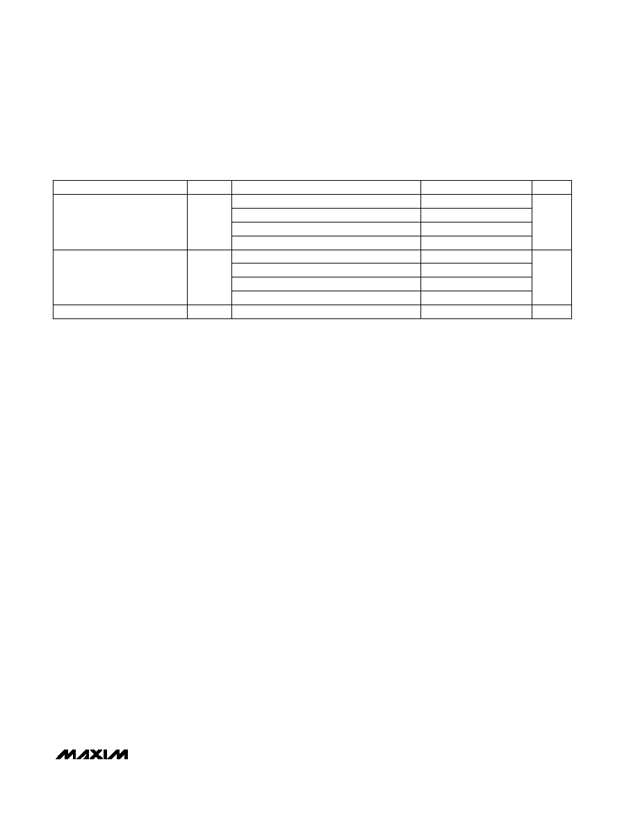
tCONV
Exiting shutdown
ms
20
Startup Time
Note 1:
AVDD = +5V, AVSS = -5V, DVDD = +5V, VREFIN = 2.500V (external), VIN = ±5V (MAX115) or ±2.5V (MAX116).
Note 2:
Integral nonlinearity is the analog value’s deviation at any code from its theoretical value after the full-scale range and
offset have been calibrated.
Note 3:
CLK synchronized with CONVST.
Note 4:
fIN = 10.06kHz, VIN = ±5V (MAX115) or ±2.5V (MAX116).
Note 5:
First five harmonics.
Note 6:
All inputs except CH1A driven with ±5V (MAX115) or ±2.5V (MAX116) 10.06kHz signal, CH1A connected to AGND and digi-
tized.
Note 7:
AVDD = DVDD = +5V, AVSS = -5V, VIN = 0V (all channels).
Note 8:
Temperature drift is defined as the change in output voltage from +25°C to TMIN or TMAX. It is calculated as
TC = [
REFOUT/REFOUT] / T.
Note 9:
See Figure 2.
Note 10: Defined as the change in positive full scale caused by a ±5% variation in the nominal supply voltage. Tested with one input
at full scale and all others at AGND. VREFIN = +2.5V (internal).
Note 11: Tested with all inputs connected to AGND. VREFIN = +2.5V (internal).
Note 12: The data access time is defined as the time required for an output to cross +0.8V or +2.0V. It is measured using the circuit
of Figure 1. The measured number is then extrapolated back to determine the value with a 25pF load.
Note 13: The bus relinquish time is derived from the measured time taken for the data outputs to change +0.5V when loaded with the
circuit of Figure 1. The measured number is then extrapolated back to remove the effects of charging and discharging the
120pF capacitor. The time given is the part’s true bus relinquish time, which is independent of the external bus loading capac-
itance.
Conversion Time
Mode 1, Channel 1
ksps
390
Conversion Rate
Mode 2, Channel 2
218
Mode 3, Channel 3
152
Mode 4, Channel 4
116
相关PDF资料 |
PDF描述 |
|---|---|
| PCM18XD1 | MODULE PIC18F248/258/448/458 |
| LGN2H101MELB25 | CAP ALUM 100UF 500V 20% SNAP |
| GSC13DREI | CONN EDGECARD 26POS .100 EYELET |
| MAX117EVKIT-DIP | EVAL KIT FOR MAX117 |
| VE-B2Z-EW | CONVERTER MOD DC/DC 2V 40W |
相关代理商/技术参数 |
参数描述 |
|---|---|
| MAX115-MAX116 | 制造商:MAXIM 制造商全称:Maxim Integrated Products 功能描述:2x4-Channel, Simultaneous-Sampling 12-Bit ADCs |
| MAX116 | 制造商:MAXIM 制造商全称:Maxim Integrated Products 功能描述:2x4-Channel, Simultaneous-Sampling 12-Bit ADCs |
| MAX1160 | 制造商:MAXIM 制造商全称:Maxim Integrated Products 功能描述:10-Bit, 20Msps, TTL-Output ADC |
| MAX11600 | 制造商:MAXIM 制造商全称:Maxim Integrated Products 功能描述:2.7V to 3.6V and 4.5V to 5.5V, Low-Power, 4-/8-/12-Channel 2-Wire Serial 8-Bit ADCs |
| MAX11600_10 | 制造商:MAXIM 制造商全称:Maxim Integrated Products 功能描述:Evaluation System |
发布紧急采购,3分钟左右您将得到回复。