- 您现在的位置:买卖IC网 > PDF目录2008 > MAX11602EEE+ (Maxim Integrated Products)IC ADC SERIAL 8BIT 8CH 16-QSOP PDF资料下载
参数资料
| 型号: | MAX11602EEE+ |
| 厂商: | Maxim Integrated Products |
| 文件页数: | 3/23页 |
| 文件大小: | 0K |
| 描述: | IC ADC SERIAL 8BIT 8CH 16-QSOP |
| 产品培训模块: | MAX116xx Lead (SnPb) Finish for COTS Obsolescence Mitigation Program |
| 标准包装: | 100 |
| 位数: | 8 |
| 采样率(每秒): | 188k |
| 数据接口: | I²C,串行 |
| 转换器数目: | 1 |
| 功率耗散(最大): | 1.75mW |
| 电压电源: | 单电源 |
| 工作温度: | -40°C ~ 85°C |
| 安装类型: | 表面贴装 |
| 封装/外壳: | 16-SSOP(0.154",3.90mm 宽) |
| 供应商设备封装: | 16-QSOP |
| 包装: | 管件 |
| 输入数目和类型: | 8 个单端,单极;8 个单端,双极;4 个差分,单极;4 个差分,双极 |
| 产品目录页面: | 1398 (CN2011-ZH PDF) |
Single-Ended/Pseudo-Differential Input
The SGL/DIF bit of the configuration byte configures the
MAX11600–MAX11605 analog input circuitry for single-
ended or pseudo-differential inputs (Table 2). In single-
ended mode (SGL/DIF = 1), the digital conversion results
are the difference between the analog input selected by
CS[3:0] and GND (Table 3). In pseudo-differential mode
(SGL/DIF = 0), the digital conversion results are the differ-
ence between the positive and the negative analog inputs
selected by CS[3:0] (Table 4). The negative analog input
signal must remain stable within ±0.5 LSB (±0.1 LSB for
best results) with respect to GND during a conversion.
Unipolar/Bipolar
When operating in pseudo-differential mode, the BIP/
UNI bit of the setup byte (Table 1) selects unipolar or
bipolar operation. Unipolar mode sets the differential
analog input range from zero to VREF. A negative differ-
ential analog input in unipolar mode causes the digital
output code to be zero. Selecting bipolar mode sets the
differential input range to ±VREF/2, with respect to the
negative input. The digital output code is binary in
unipolar mode and two’s complement binary in bipolar
mode (see the
Transfer Functions section).
In single-ended mode, the MAX11600–MAX11605
always operate in unipolar mode regardless of the
BIP/UNI setting, and the analog inputs are internally ref-
erenced to GND with a full-scale input range from zero
to VREF.
Digital Interface
The MAX11600–MAX11605 feature a 2-wire interface
consisting of a serial-data line (SDA) and a serial-clock
line (SCL). SDA and SCL facilitate bidirectional communi-
cation between the MAX11600–MAX11605 and the mas-
ter at rates up to 1.7MHz. The MAX11600–MAX11605 are
slaves that transmit and receive data. The master (typical-
ly a microcontroller) initiates data transfer on the bus and
generates SCL to permit that transfer.
SDA and SCL must be pulled high. This is typically
done with pullup resistors (500
or greater) (see
Typical Operating Circuit). Series resistors (RS) are
optional. They protect the input architecture of the
MAX11600–MAX11605 from high-voltage spikes on the
bus lines and minimize crosstalk and undershoot of the
bus signals.
Bit Transfer
One data bit is transferred during each SCL clock
cycle. Nine clock cycles are required to transfer the
data in or out of the MAX11600–MAX11605. The data
on SDA must remain stable during the high period of
the SCL clock pulse. Changes in SDA while SCL is high
are control signals (see the
START and STOP
Conditions section). Both SDA and SCL idle high when
the bus is not busy.
START and STOP Conditions
The master initiates a transmission with a START condi-
tion (S), a high-to-low transition on SDA with SCL high.
The master terminates a transmission with a STOP
condition (P), a low-to-high transition on SDA, while
MAX11600–MAX11605
2.7V to 3.6V and 4.5V to 5.5V, Low-Power,
4-/8-/12-Channel 2-Wire Serial 8-Bit ADCs
______________________________________________________________________________________
11
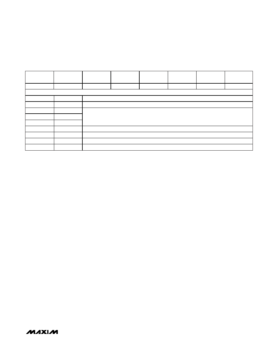
BIT 7
(MSB)
BIT 6
BIT 5
BIT 4
BIT 3
BIT 2
BIT 1
BIT 0
(LSB)
REG
SEL2
SEL1
SEL0
CLK
BIP/
UNI
RST
X
BIT
NAME
DESCRIPTION
7
REG
Register bit. 1 = setup byte, 0 = configuration byte (Table 2).
6
SEL2
5
SEL1
4
SEL0
Three bits select the reference voltage and the state of AIN_/REF
(MAX11600/MAX11601/MAX11604/MAX11605) or REF (MAX11602/MAX11603) (Table 6).
Default to 000 at power-up.
3
CLK
1 = external clock, 0 = internal clock. Defaulted to zero at power-up.
2
BIP/
UNI
1 = bipolar, 0 = unipolar. Defaulted to zero at power-up (see the Unipolar/Bipolar section).
1
RST
1 = no action, 0 = resets the configuration register to default. Setup register remains unchanged.
0
X
Don’t care; can be set to 1 or 0.
Table 1. Setup Byte Format
相关PDF资料 |
PDF描述 |
|---|---|
| MAX11610EEE+T | IC ADC SERIAL 10BIT 12CH 16-QSOP |
| MAX11616EEE+T | IC ADC SERIAL 12BIT 12CH 16-QSOP |
| MAX1162AEUB+T | IC ADC 16BIT 200KSPS 10-MSOP |
| MAX11637EEE+T | IC ADC 12BIT 8CH 16QSOP |
| MAX11643EEG+T | IC ADC 8BIT 8CH 24QSOP |
相关代理商/技术参数 |
参数描述 |
|---|---|
| MAX11602EEE+ | 功能描述:模数转换器 - ADC 8-Bit 8Ch 188ksps 5.5V Precision ADC RoHS:否 制造商:Texas Instruments 通道数量:2 结构:Sigma-Delta 转换速率:125 SPs to 8 KSPs 分辨率:24 bit 输入类型:Differential 信噪比:107 dB 接口类型:SPI 工作电源电压:1.7 V to 3.6 V, 2.7 V to 5.25 V 最大工作温度:+ 85 C 安装风格:SMD/SMT 封装 / 箱体:VQFN-32 |
| MAX11602EEE+T | 功能描述:模数转换器 - ADC 8-Bit 8Ch 188ksps 5.5V Precision ADC RoHS:否 制造商:Texas Instruments 通道数量:2 结构:Sigma-Delta 转换速率:125 SPs to 8 KSPs 分辨率:24 bit 输入类型:Differential 信噪比:107 dB 接口类型:SPI 工作电源电压:1.7 V to 3.6 V, 2.7 V to 5.25 V 最大工作温度:+ 85 C 安装风格:SMD/SMT 封装 / 箱体:VQFN-32 |
| MAX11603 | 制造商:MAXIM 制造商全称:Maxim Integrated Products 功能描述:2.7V to 3.6V and 4.5V to 5.5V, Low-Power, 4-/8-/12-Channel 2-Wire Serial 8-Bit ADCs |
| MAX11603EEE+ | 功能描述:模数转换器 - ADC 8-Bit 8Ch 188ksps 3.6V Precision ADC RoHS:否 制造商:Texas Instruments 通道数量:2 结构:Sigma-Delta 转换速率:125 SPs to 8 KSPs 分辨率:24 bit 输入类型:Differential 信噪比:107 dB 接口类型:SPI 工作电源电压:1.7 V to 3.6 V, 2.7 V to 5.25 V 最大工作温度:+ 85 C 安装风格:SMD/SMT 封装 / 箱体:VQFN-32 |
| MAX11603EEE+T | 功能描述:模数转换器 - ADC 8-Bit 8Ch 188ksps 3.6V Precision ADC RoHS:否 制造商:Texas Instruments 通道数量:2 结构:Sigma-Delta 转换速率:125 SPs to 8 KSPs 分辨率:24 bit 输入类型:Differential 信噪比:107 dB 接口类型:SPI 工作电源电压:1.7 V to 3.6 V, 2.7 V to 5.25 V 最大工作温度:+ 85 C 安装风格:SMD/SMT 封装 / 箱体:VQFN-32 |
发布紧急采购,3分钟左右您将得到回复。