- 您现在的位置:买卖IC网 > PDF目录383311 > MAX1160ACPI (MAXIM INTEGRATED PRODUCTS INC) 10-Bit, 20Msps, TTL-Output ADC PDF资料下载
参数资料
| 型号: | MAX1160ACPI |
| 厂商: | MAXIM INTEGRATED PRODUCTS INC |
| 元件分类: | ADC |
| 英文描述: | 10-Bit, 20Msps, TTL-Output ADC |
| 中文描述: | 1-CH 10-BIT PROPRIETARY METHOD ADC, PARALLEL ACCESS, PDIP28 |
| 封装: | 0.600 INCH, PLASTIC, DIP-28 |
| 文件页数: | 7/8页 |
| 文件大小: | 76K |
| 代理商: | MAX1160ACPI |
M
10-Bit, 20Msps, T T L-Output ADC
_______________________________________________________________________________________
7
COARSE
ADC
SUCCESSIVE
INTERPOLATION
STAGE 1
SUCCESSIVE
INTERPOLATION
STAGE N
ANALOG
PRESCALER
DIGITAL
OUTPUTS
D
V
E
V
E
A
A
V
C
V
C
D
C
D
C
D
D
FB
F
F
+5V
-5.2V
+5V
R1
10k
R2
30k
R3
30k
R4
10k
1
μ
F
0.01
μ
F
0.01
μ
F
1
μ
F
10
μ
F
10
μ
F
1
μ
F
C1
0.01
μ
F
C2
0.01
μ
F
C3
0.01
μ
F
C4
0.01
μ
F
C6
0.1
μ
F
C7
0.1
μ
F
C8
0.1
μ
F
C9
0.1
μ
F
C10
0.01
μ
F
C11
0.01
μ
F
C5
0.01
μ
F
VIN
(±2V)
±2.5V MAX
CLK
(TTL)
VIN
VFT
VIN
CLK
VST
VRM
VSB
VFB
GND
VOUT
VTRIM
R5
100
2.5V
1
3
2
4
6
7
8
R
2R
2R
2R
2R
R
D1
-5.2V
= AGND
+5V
= DGND
D10
D9
D8
D7
D6
D5
D4
D3
D2
D1
D0
2
4
5
6
NOTES:
1) D1 = SCHOTTKY OR HOT CARRIER DIODE
2) FB = FERRITE BEAD, FAIR RITE #2743001111
TOBE MOUNTED AS CLOSELY TOTHE DEVICE
AS POSSIBLE. THE FERRITE BEAD TOADC
CONNECTION SHOULD NOT BE SHARED WITH
ANY OTHER DEVICE.
3) C1–C11 = CHIP CAPACITOR (RECOMMENDED)
MOUNTED AS CLOSE TODEVICE'S PIN AS
POSSIBLE.
4) USE OF A SEPARATE SUPPLY FOR V
CC
AND DV
CC
IS NOT RECOMMENDED.
5) R5 PROVIDES CURRENT LIMITING TO45mA.
(OVERRANGE)
(MSB)
(LSB)
4
-2.5V
MAX1160
IC1
IC2
OP07
MAX6225
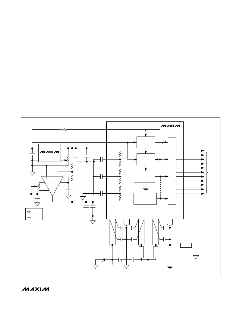
Figure 2. Typical Operating Circuit
The following errors are defined:
+FS error = top of ladder offset voltage
=
(+FS - VST + 1LSB)
-FS error = bottom of ladder offset voltage
=
(-FS - VSB - 1LSB)
where the +FS (full-scale) input voltage is defined as the
output transition between 11 1111 1110 and 11 1111 1111,
and the -FS input voltage is defined as the output transi-
tion between 00 0000 0000 and 00 0000 0001 (Table 2).
Analog Input
VIN is the analog input. The full-scale input range will
be 80% of the reference voltage, or ±2V with VFB =
-2.5V and VFT = +2.5V.
The analog input’s drive requirements are minimal
when compared to conventional flash converters. This
is due to the MAX1160’s extremely low (5pF) input
capacitance and very high (300k
) input resistance.
For example, for an input signal of ±2Vp-p with a
10MHz input frequency, the peak output current
required for the driving circuit is only 628μA.
Cloc k Input
The MAX1160 is driven from a single-ended TTL input
(CLK). The CLK pulse width (t
pwH
) must be kept
between 20ns and 300ns to ensure proper operation of
the internal track/hold amplifier (Figure 1a). When oper-
ating the MAX1160 at sampling rates above 3Msps, it is
recommended that the clock input duty cycle be kept at
相关PDF资料 |
PDF描述 |
|---|---|
| MAX1160 | Low-Voltage Adjustable Precision Shunt Regulator 3-SOT-23 -40 to 85 |
| MAX1160ACWI | 10-Bit, 20Msps, TTL-Output ADC |
| MAX1160BCPI | 10-Bit, 20Msps, TTL-Output ADC |
| MAX1160BCWI | 10-Bit, 20Msps, TTL-Output ADC |
| MAX1168AEEG | Multichannel, 16-Bit, 200ksps Analog-to-Digital Converters |
相关代理商/技术参数 |
参数描述 |
|---|---|
| MAX1160ACWI | 制造商:MAXIM 制造商全称:Maxim Integrated Products 功能描述:10-Bit, 20Msps, TTL-Output ADC |
| MAX1160BCPI | 制造商:MAXIM 制造商全称:Maxim Integrated Products 功能描述:10-Bit, 20Msps, TTL-Output ADC |
| MAX1160BCWI | 制造商:MAXIM 制造商全称:Maxim Integrated Products 功能描述:10-Bit, 20Msps, TTL-Output ADC |
| MAX1161 | 制造商:MAXIM 制造商全称:Maxim Integrated Products 功能描述:10-Bit, 40Msps, TTL-Output ADC |
| MAX11610 | 制造商:MAXIM 制造商全称:Maxim Integrated Products 功能描述:2.7V to 3.6V and 4.5V to 5.5V, Low-Power, 4-/8-/12-Channel, 2-Wire Serial 10-Bit ADCs |
发布紧急采购,3分钟左右您将得到回复。