- 您现在的位置:买卖IC网 > PDF目录9964 > MAX11615EEE+T (Maxim Integrated Products)IC ADC SERIAL 12BIT 8CH 16-QSOP PDF资料下载
参数资料
| 型号: | MAX11615EEE+T |
| 厂商: | Maxim Integrated Products |
| 文件页数: | 8/24页 |
| 文件大小: | 0K |
| 描述: | IC ADC SERIAL 12BIT 8CH 16-QSOP |
| 产品培训模块: | Lead (SnPb) Finish for COTS Obsolescence Mitigation Program |
| 标准包装: | 2,500 |
| 位数: | 12 |
| 采样率(每秒): | 94.4k |
| 数据接口: | I²C,串行 |
| 转换器数目: | 1 |
| 功率耗散(最大): | 666.7mW |
| 电压电源: | 单电源 |
| 工作温度: | -40°C ~ 85°C |
| 安装类型: | 表面贴装 |
| 封装/外壳: | 16-SSOP(0.154",3.90mm 宽) |
| 供应商设备封装: | 16-QSOP |
| 包装: | 带卷 (TR) |
| 输入数目和类型: | 8 个单端,单极;8 个单端,双极;4 个差分,单极;4 个差分,双极 |
MAX11612–MAX11617
Low-Power, 4-/8-/12-Channel, I2C,
12-Bit ADCs in Ultra-Small Packages
16
Maxim Integrated
Data Byte (Read Cycle)
A read cycle must be initiated to obtain conversion
results. Read cycles begin with the bus master issuing
a START condition followed by seven address bits and
a read bit (R/W = 1). If the address byte is successfully
received, the MAX11612–MAX11617 (slave) issues an
acknowledge. The master then reads from the slave.
The result is transmitted in two bytes; first four bits of
the first byte are high, then MSB through LSB are con-
secutively clocked out. After the master has received
the byte(s), it can issue an acknowledge if it wants to
continue reading or a not-acknowledge if it no longer
wishes to read. If the MAX11612–MAX11617 receive a
not-acknowledge, they release SDA, allowing the master
to generate a STOP or a repeated START condition. See
the
Clock Modes and Scan Mode sections for detailed
information on how data is obtained and converted.
Clock Modes
The clock mode determines the conversion clock and
the data acquisition and conversion time. The clock
mode also affects the scan mode. The state of the set-
up byte’s CLK bit determines the clock mode (Table 1).
At power-up, the MAX11612–MAX11617 are defaulted
to internal clock mode (CLK = 0).
Internal Clock
When configured for internal clock mode (CLK = 0), the
MAX11612–MAX11617 use their internal oscillator as the
conversion clock. In internal clock mode, the MAX11612–
MAX11617 begin tracking the analog input after a valid
address on the eighth rising edge of the clock. On the
falling edge of the ninth clock, the analog signal is acquired
and the conversion begins. While converting the analog
input signal, the MAX11612–MAX11617 holds SCL low
(clock stretching). After the conversion completes, the
results are stored in internal memory. If the scan mode is set
for multiple conversions, they all happen in succession with
each additional result stored in memory. The MAX11612/
MAX11613 contain four 12-bit blocks of memory, the
MAX11614/MAX11615 contain eight 12-bit blocks of memo-
ry, and the MAX11616/MAX11617 contain twelve 12-bit
blocks of memory. Once all conversions are complete, the
MAX11612–MAX11617 release SCL, allowing it to be pulled
high. The master can now clock the results out of the mem-
ory in the same order the scan conversion has been done
at a clock rate of up to 1.7MHz. SCL is stretched for a maxi-
mum of 8.3s per channel (see Figure 10).
The device memory contains all of the conversion
results when the MAX11612–MAX11617 release SCL.
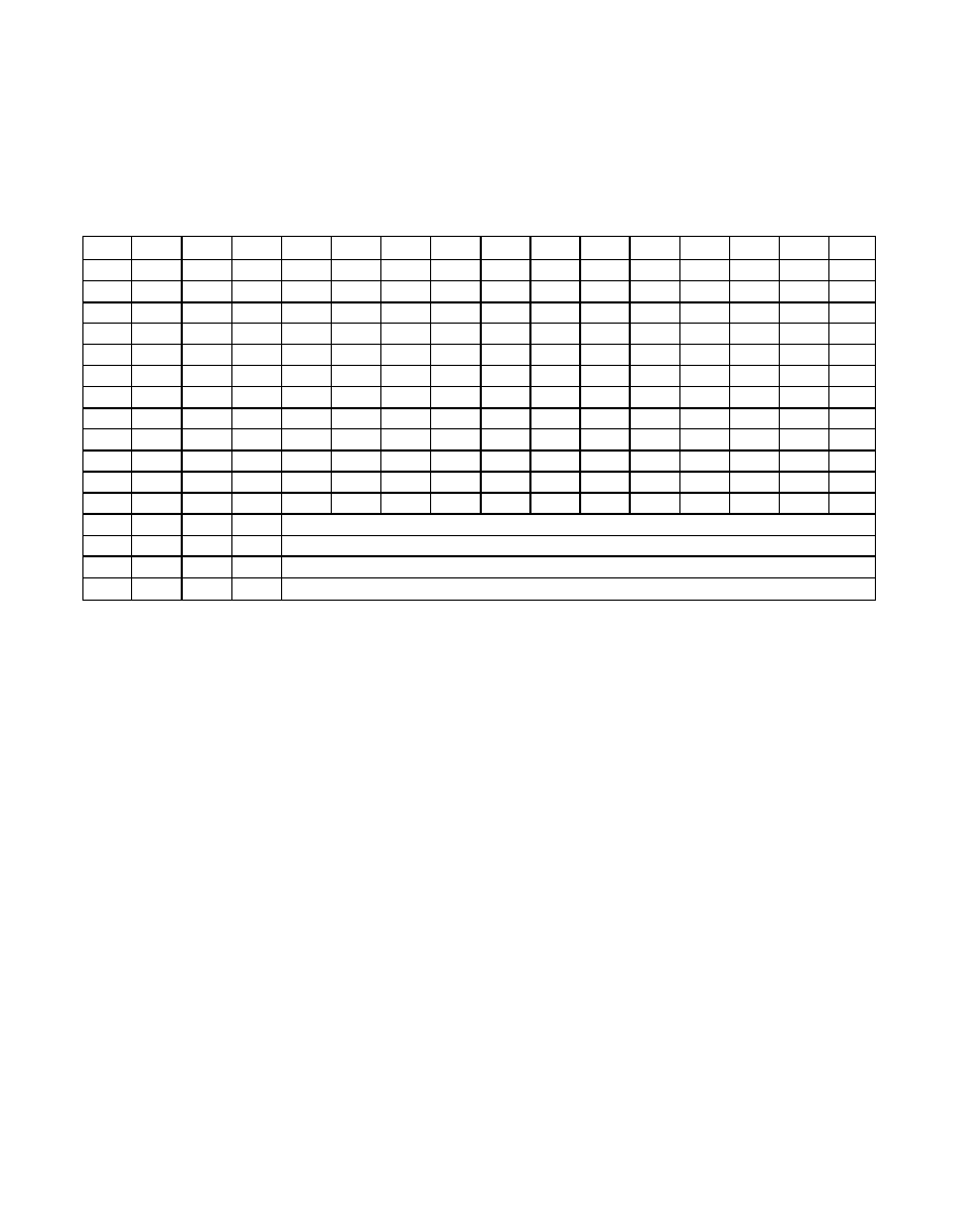
CS3
1
CS2
1
CS1
CS0
AIN0
AIN1
AIN2
AIN3
2
AIN4
AIN5
AIN6
AIN7
AIN8
AIN9
AIN10 AIN11
2
0000
+
-
0001
-
+
0010
+
-
0011
-
+
0100
+
-
0101
-
+
0110
+
-
0111
-
+
1000
+-
1001
-+
1010
+-
1011
-+
1100
RESERVED
1101
RESERVED
1110
RESERVED
1111
RESERVED
1For the MAX11612/MAX11613, CS3 and CS2 are internally set to 0. For the MAX11614/MAX11615, CS3 is internally set to 0.
2When SEL1 = 1, a differential read between AIN2 and AIN3/REF (MAX11612/MAX11613) or AIN10 and AIN11/REF
(MAX11616/MAX11617) returns the difference between GND and AIN2 or AIN10, respectively. For example, a differential read of 1011
returns the negative difference between AIN10 and GND. This does not apply to the MAX11614/MAX11615 as each provides separate
pins for AIN7 and REF. In differential scanning, the address increments by 2 until the limit set by CS3–CS1 has been reached.
Table 4. Channel Selection in Differential Mode (SGL/
DIF = 0)
相关PDF资料 |
PDF描述 |
|---|---|
| VE-21F-MX-F1 | CONVERTER MOD DC/DC 72V 75W |
| VI-25D-IX-B1 | CONVERTER MOD DC/DC 85V 75W |
| V48B36M250BF | CONVERTER MOD DC/DC 36V 250W |
| VE-21D-MX-F3 | CONVERTER MOD DC/DC 85V 75W |
| HIN232EIVZ-T | IC 2DRVR/2RCVR RS232 5V 16-TSSOP |
相关代理商/技术参数 |
参数描述 |
|---|---|
| MAX11615EVKIT+ | 功能描述:数据转换 IC 开发工具 MAX11615 Eval Kit RoHS:否 制造商:Texas Instruments 产品:Demonstration Kits 类型:ADC 工具用于评估:ADS130E08 接口类型:SPI 工作电源电压:- 6 V to + 6 V |
| MAX11615EVSYS+ | 功能描述:数据转换 IC 开发工具 MAX11615 Eval Kit RoHS:否 制造商:Texas Instruments 产品:Demonstration Kits 类型:ADC 工具用于评估:ADS130E08 接口类型:SPI 工作电源电压:- 6 V to + 6 V |
| MAX11615EWE+ | 制造商:Maxim Integrated Products 功能描述:2.7V TO 3.6V, LOW-POWER, 8-CHANNEL, 2-WIRE SERIAL 12-BIT ADC - Rail/Tube |
| MAX11615EWE+T | 功能描述:模数转换器 - ADC 12Bit 8Ch 94.4ksps ADC RoHS:否 制造商:Texas Instruments 通道数量:2 结构:Sigma-Delta 转换速率:125 SPs to 8 KSPs 分辨率:24 bit 输入类型:Differential 信噪比:107 dB 接口类型:SPI 工作电源电压:1.7 V to 3.6 V, 2.7 V to 5.25 V 最大工作温度:+ 85 C 安装风格:SMD/SMT 封装 / 箱体:VQFN-32 |
| MAX11616 | 制造商:MAXIM 制造商全称:Maxim Integrated Products 功能描述:2.7V to 3.6V and 4.5V to 5.5V, Low-Power, 4-/8-/12-Channel, 2-Wire Serial, 12-Bit ADCs |
发布紧急采购,3分钟左右您将得到回复。