- 您现在的位置:买卖IC网 > PDF目录17021 > MAX11617EVSYS+ (Maxim Integrated Products)EVALUATION SYSTEM FOR MAX11617 PDF资料下载
参数资料
| 型号: | MAX11617EVSYS+ |
| 厂商: | Maxim Integrated Products |
| 文件页数: | 10/24页 |
| 文件大小: | 0K |
| 描述: | EVALUATION SYSTEM FOR MAX11617 |
| 产品培训模块: | Lead (SnPb) Finish for COTS Obsolescence Mitigation Program |
| 标准包装: | 1 |
| ADC 的数量: | 1 |
| 位数: | 8,10,12 |
| 采样率(每秒): | 94.4k |
| 数据接口: | I²C,串行 |
| 工作温度: | -40°C ~ 85°C |
| 已用 IC / 零件: | MAX11617 |
| 已供物品: | 2 个板,软件 |
MAX11612–MAX11617
Low-Power, 4-/8-/12-Channel, I2C,
12-Bit ADCs in Ultra-Small Packages
18
Maxim Integrated
converted data is available immediately after the first
four empty high bits. The device continuously converts
input channels dictated by the scan mode until given a
not acknowledge. There is no need to readdress the
device with a read command to obtain new conversion
results (see Figure 11).
The conversion must complete in 1ms, or droop on the
track-and-hold capacitor degrades conversion results.
Use internal clock mode if the SCL clock period
exceeds 60s.
The MAX11612–MAX11617 must operate in external
clock mode for conversion rates from 40ksps to
94.4ksps. Below 40ksps, internal clock mode is recom-
mended due to much smaller power consumption.
Scan Mode
SCAN0 and SCAN1 of the configuration byte set the
scan mode configuration. Table 5 shows the scanning
configurations. If AIN_/REF is set to be a reference input
or output (SEL1 = 1, Table 6), AIN_/REF is excluded from
a multichannel scan. The scanned results are written to
memory in the same order as the conversion. Read the
results from memory in the order they were converted.
Each result needs a 2-byte transmission; the first byte
begins with four empty bits, during which SDA is left
high. Each byte has to be acknowledged by the master
or the memory transmission is terminated. It is not possi-
ble to read the memory independently of conversion.
Applications Information
Power-On Reset
The configuration and setup registers (Tables 1 and 2)
default to a single-ended, unipolar, single-channel con-
version on AIN0 using the internal clock with VDD as the
reference and AIN_/REF configured as an analog input.
The memory contents are unknown after power-up.
Automatic Shutdown
Automatic shutdown occurs between conversions when
the MAX11612–MAX11617 are idle. All analog circuits
participate in automatic shutdown except the internal
reference due to its prohibitively long wake-up time.
When operating in external clock mode, a STOP, not-
acknowledge, or repeated START condition must be
issued to place the devices in idle mode and benefit
from automatic shutdown. A STOP condition is not nec-
essary in internal clock mode to benefit from automatic
shutdown because power-down occurs once all con-
version results are written to memory (Figure 10). When
using an external reference or VDD as a reference, all
analog circuitry is inactive in shutdown and supply cur-
rent is less than 0.5A. The digital conversion results
obtained in internal clock mode are maintained in memo-
ry during shutdown and are available for access through
the serial interface at any time prior to a STOP or a
repeated START condition.
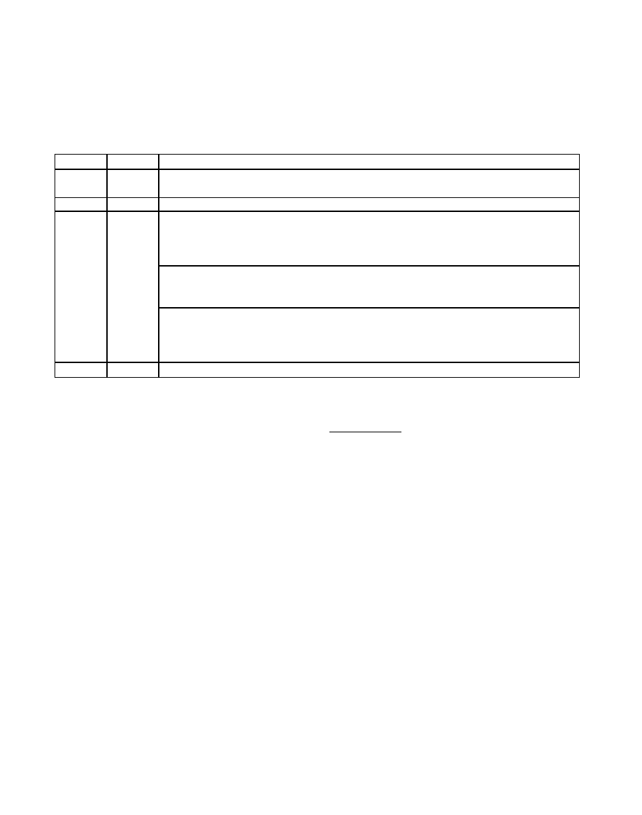
SCAN1
SCAN0
SCANNING CONFIGURATION
00
Scans up from AIN0 to the input selected by CS3–CS0. When CS3–CS0 exceeds 1011, the scanning
stops at AIN11. When AIN_/REF is set to be a REF input/output, scanning stops at AIN2 or AIN10.
0
1
*Converts the input selected by CS3–CS0 eight times (see Tables 3 and 4).
MAX11612/MAX11613: Scans upper half of channels.
Scans up from AIN2 to the input selected by CS1 and CS0. When CS1 and CS0 are set for AIN0, AIN1,
and AIN2, the only scan that takes place is AIN2 (MAX11612/MAX11613). When AIN/REF is set to be a
REF input/output, scanning stops at AIN2.
MAX11614/MAX11615: Scans upper quartile of channels.
Scans up from AIN6 to the input selected by CS3–CS0. When CS3–CS0 is set for AIN0–AIN6, the only
scan that takes place is AIN6 (MAX11614/MAX11615).
10
MAX11616/MAX11617: Scans upper half of channels.
Scans up from AIN6 to the input selected by CS3–CS0. When CS3–CS0 is set for AIN0–AIN6, the only
scan that takes place is AIN6 (MAX11616/MAX11617). When AIN/REF is set to be a REF input/output,
scanning stops at selected channel or AIN10.
1
*Converts channel selected by CS3–CS0.
*
When operating in external clock mode, there is no difference between SCAN[1:0] = 01 and SCAN[1:0] = 11, and converting occurs
perpetually until not-acknowledge occurs.
Table 5. Scanning Configuration
相关PDF资料 |
PDF描述 |
|---|---|
| LLS1J472MELB | CAP ALUM 4700UF 63V 20% SNAP |
| LGU2G151MELA | CAP ALUM 150UF 400V 20% SNAP |
| VE-B5W-EY | CONVERTER MOD DC/DC 5.5V 50W |
| MAX11616EVSYS+ | EVALUATION SYSTEM FOR MAX11616 |
| FPF2104 | IC SWITCH LOAD FULL FUNC SOT23-5 |
相关代理商/技术参数 |
参数描述 |
|---|---|
| MAX11617EVSYS+ | 功能描述:数据转换 IC 开发工具 MAX11617 Eval Kit RoHS:否 制造商:Texas Instruments 产品:Demonstration Kits 类型:ADC 工具用于评估:ADS130E08 接口类型:SPI 工作电源电压:- 6 V to + 6 V |
| MAX11617EWE+ | 制造商:Maxim Integrated Products 功能描述:2.7V TO 3.6V, LOW-POWER, 12-CHANNEL, 2-WIRE SERIAL 12-BIT AD - Rail/Tube |
| MAX11617EWE+T | 功能描述:模数转换器 - ADC 12Bit 12Ch 94.4ksps ADC RoHS:否 制造商:Texas Instruments 通道数量:2 结构:Sigma-Delta 转换速率:125 SPs to 8 KSPs 分辨率:24 bit 输入类型:Differential 信噪比:107 dB 接口类型:SPI 工作电源电压:1.7 V to 3.6 V, 2.7 V to 5.25 V 最大工作温度:+ 85 C 安装风格:SMD/SMT 封装 / 箱体:VQFN-32 |
| MAX11618EEE+ | 功能描述:模数转换器 - ADC 4Ch 10-Bit 300ksps w/FIFO & Int Ref RoHS:否 制造商:Texas Instruments 通道数量:2 结构:Sigma-Delta 转换速率:125 SPs to 8 KSPs 分辨率:24 bit 输入类型:Differential 信噪比:107 dB 接口类型:SPI 工作电源电压:1.7 V to 3.6 V, 2.7 V to 5.25 V 最大工作温度:+ 85 C 安装风格:SMD/SMT 封装 / 箱体:VQFN-32 |
| MAX11618EEE+T | 功能描述:模数转换器 - ADC 4Ch 10-Bit 300ksps w/FIFO & Int Ref RoHS:否 制造商:Texas Instruments 通道数量:2 结构:Sigma-Delta 转换速率:125 SPs to 8 KSPs 分辨率:24 bit 输入类型:Differential 信噪比:107 dB 接口类型:SPI 工作电源电压:1.7 V to 3.6 V, 2.7 V to 5.25 V 最大工作温度:+ 85 C 安装风格:SMD/SMT 封装 / 箱体:VQFN-32 |
发布紧急采购,3分钟左右您将得到回复。