- 您现在的位置:买卖IC网 > PDF目录9744 > MAX1162AEUB+ (Maxim Integrated Products)IC ADC 16BIT 200KSPS 10-MSOP PDF资料下载
参数资料
| 型号: | MAX1162AEUB+ |
| 厂商: | Maxim Integrated Products |
| 文件页数: | 17/18页 |
| 文件大小: | 0K |
| 描述: | IC ADC 16BIT 200KSPS 10-MSOP |
| 标准包装: | 50 |
| 位数: | 16 |
| 采样率(每秒): | 200k |
| 数据接口: | MICROWIRE?,QSPI?,串行,SPI? |
| 转换器数目: | 1 |
| 功率耗散(最大): | 444mW |
| 电压电源: | 模拟和数字 |
| 工作温度: | -40°C ~ 85°C |
| 安装类型: | 表面贴装 |
| 封装/外壳: | 10-TFSOP,10-MSOP(0.118",3.00mm 宽) |
| 供应商设备封装: | 10-µMAX |
| 包装: | 管件 |
| 输入数目和类型: | 1 个单端,单极 |
MAX1162
16-Bit, +5V, 200ksps ADC with 10A
Shutdown
8
_______________________________________________________________________________________
Detailed Description
The MAX1162 includes an input track-and-hold (T/H)
and successive-approximation register (SAR) circuitry
to convert an analog input signal to a digital 16-bit out-
put. Figure 4 shows the MAX1162 in its simplest config-
uration. The serial interface requires only three digital
lines (SCLK, CS, and DOUT) and provides an easy
interface to microprocessors (Ps).
The MAX1162 has two power modes: normal and shut-
down. Driving CS high places the MAX1162 in shut-
down, reducing the supply current to 0.1A (typ), while
pulling CS low places the MAX1162 in normal operating
mode. Falling edges on CS initiate conversions that are
driven by SCLK. The conversion result is available at
DOUT in unipolar serial format. The serial data stream
consists of eight zeros followed by the data bits (MSB
first). Figure 3 shows the interface timing diagram.
Analog Input
Figure 5 illustrates the input sampling architecture of
the ADC. The voltage applied at REF sets the full-scale
input voltage.
Track-and-Hold (T/H)
In track mode, the analog signal is acquired on the
internal hold capacitor. In hold mode, the T/H switches
open and the capacitive DAC samples the analog input.
During the acquisition, the analog input (AIN) charges
capacitor CDAC. The acquisition interval ends on the
falling edge of the sixth clock cycle (Figure 6). At this
instant, the T/H switches open. The retained charge on
CDAC represents a sample of the input.
In hold mode, the capacitive digital-to-analog converter
(DAC) adjusts during the remainder of the conversion
cycle to restore node ZERO to zero within the limits of
16-bit resolution. At the end of the conversion, force CS
high and then low to reset the input side of the CDAC
switches back to AIN, and charge CDAC to the input
signal again.
The time required for the T/H to acquire an input signal
is a function of how quickly its input capacitance is
charged. If the input signal’s source impedance is high,
the acquisition time lengthens and more time must be
allowed between conversions. The acquisition time
(tACQ) is the maximum time the device takes to acquire
the signal. Use the following formula to calculate acqui-
sition time:
tACQ = 13(RS + RIN) x 35pF
where RIN = 800, RS = the input signal’s source
impedance, and tACQ is never less than 1.1s. A
source impedance less than 1k
does not significantly
affect the ADC’s performance.
To improve the input signal bandwidth under AC condi-
tions, drive AIN with a wideband buffer (>4MHz) that can
drive the ADC’s input capacitance and settle quickly.
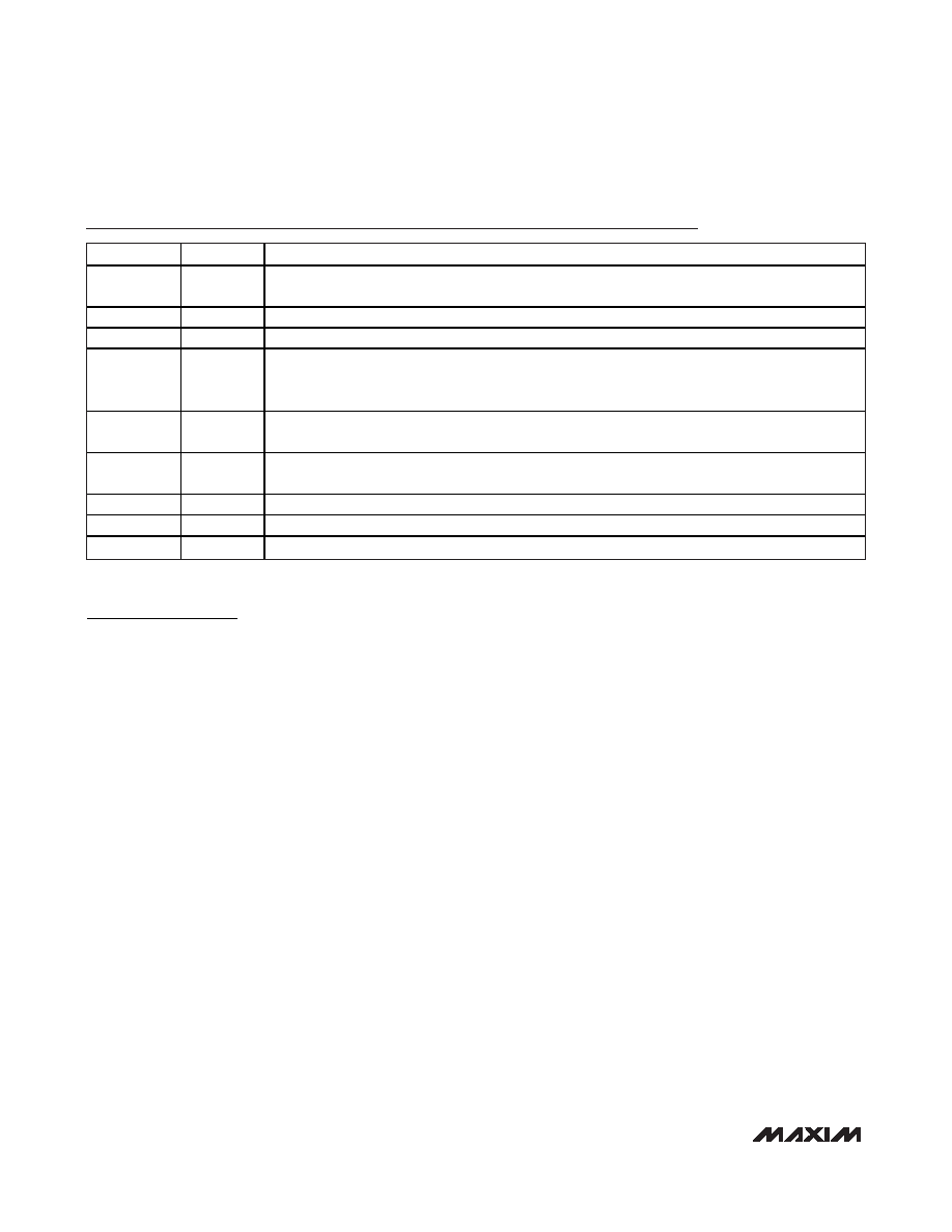
Pin Description
PIN
NAME
FUNCTION
1
REF
External Reference Voltage Input. Sets the analog voltage range. Bypass to AGND with a 4.7F
capacitor.
2AVDD
Analog +5V Supply Voltage. Bypass to AGND (pin 3) with a 0.1F capacitor.
3, 9
AGND
Analog Ground. Connect pins 3 and 9 together. Place star ground at pin 3.
4
CS
Active-Low Chip-Select Input. Forcing
CS high places the MAX1162 in shutdown with a typical
current of 0.1A. A high-to-low transition on
CS activates normal operating mode and initiates a
conversion.
5
SCLK
Serial Clock Input. SCLK drives the conversion process and clocks out data at data rates up to
4.8MHz.
6DOUT
Serial Data Output. Data changes state on SCLK’s falling edge. DOUT is high impedance when
CS
is high.
7
DGND
Digital Ground
8DVDD
Digital Supply Voltage. Bypass to DGND with a 0.1F capacitor.
10
AIN
Analog Input
相关PDF资料 |
PDF描述 |
|---|---|
| MS27474T8A35SA | CONN RCPT 6POS JAM NUT W/SCKT |
| VI-J1M-MX-F2 | CONVERTER MINIMOD DC/DC 10V 75W |
| D38999/20JD19JN | CONN RCPT 19POS WALL MNT W/SCKT |
| VI-J1M-MX-F1 | CONVERTER MINIMOD DC/DC 10V 75W |
| MS27505E25B35P | CONN RCPT 128POS BOX MNT W/PINS |
相关代理商/技术参数 |
参数描述 |
|---|---|
| MAX1162AEUB+ | 功能描述:模数转换器 - ADC RoHS:否 制造商:Texas Instruments 通道数量:2 结构:Sigma-Delta 转换速率:125 SPs to 8 KSPs 分辨率:24 bit 输入类型:Differential 信噪比:107 dB 接口类型:SPI 工作电源电压:1.7 V to 3.6 V, 2.7 V to 5.25 V 最大工作温度:+ 85 C 安装风格:SMD/SMT 封装 / 箱体:VQFN-32 |
| MAX1162AEUB+T | 功能描述:模数转换器 - ADC RoHS:否 制造商:Texas Instruments 通道数量:2 结构:Sigma-Delta 转换速率:125 SPs to 8 KSPs 分辨率:24 bit 输入类型:Differential 信噪比:107 dB 接口类型:SPI 工作电源电压:1.7 V to 3.6 V, 2.7 V to 5.25 V 最大工作温度:+ 85 C 安装风格:SMD/SMT 封装 / 箱体:VQFN-32 |
| MAX1162AEUB-T | 功能描述:模数转换器 - ADC RoHS:否 制造商:Texas Instruments 通道数量:2 结构:Sigma-Delta 转换速率:125 SPs to 8 KSPs 分辨率:24 bit 输入类型:Differential 信噪比:107 dB 接口类型:SPI 工作电源电压:1.7 V to 3.6 V, 2.7 V to 5.25 V 最大工作温度:+ 85 C 安装风格:SMD/SMT 封装 / 箱体:VQFN-32 |
| MAX1162BC_B | 制造商:MAXIM 制造商全称:Maxim Integrated Products 功能描述:16-Bit, +5V, 200ksps ADC with 10レA Shutdown |
| MAX1162BCUB | 功能描述:模数转换器 - ADC RoHS:否 制造商:Texas Instruments 通道数量:2 结构:Sigma-Delta 转换速率:125 SPs to 8 KSPs 分辨率:24 bit 输入类型:Differential 信噪比:107 dB 接口类型:SPI 工作电源电压:1.7 V to 3.6 V, 2.7 V to 5.25 V 最大工作温度:+ 85 C 安装风格:SMD/SMT 封装 / 箱体:VQFN-32 |
发布紧急采购,3分钟左右您将得到回复。