参数资料
| 型号: | MAX11643EEG+T |
| 厂商: | Maxim Integrated Products |
| 文件页数: | 4/22页 |
| 文件大小: | 0K |
| 描述: | IC ADC 8BIT 8CH 24QSOP |
| 产品培训模块: | Lead (SnPb) Finish for COTS Obsolescence Mitigation Program |
| 标准包装: | 2,500 |
| 位数: | 8 |
| 采样率(每秒): | 300k |
| 数据接口: | MICROWIRE?,QSPI?,串行,SPI? |
| 转换器数目: | 1 |
| 功率耗散(最大): | 762mW |
| 电压电源: | 单电源 |
| 工作温度: | -40°C ~ 85°C |
| 安装类型: | 表面贴装 |
| 封装/外壳: | 24-SSOP(0.154",3.90mm 宽) |
| 供应商设备封装: | 24-QSOP |
| 包装: | 带卷 (TR) |
| 输入数目和类型: | 16 个单端,单极 |
MAX11638/MAX11639/MAX11642/MAX11643
8-Bit, 16-/8-Channel, 300ksps ADCs
with FIFO and Internal Reference
12
______________________________________________________________________________________
Converter Operation
The MAX11638/MAX11639/MAX11642/MAX11643 ADCs
use a successive-approximation register (SAR) conver-
sion technique and an on-chip T/H block to convert
voltage signals into an 8-bit digital result. This single-
ended configuration supports unipolar signal ranges.
Input Bandwidth
The ADC’s input-tracking circuitry has a 1MHz small-
signal bandwidth, so it is possible to digitize high-speed
transient events and measure periodic signals with
bandwidths exceeding the ADC’s sampling rate by
using undersampling techniques. Anti-alias prefiltering
of the input signals is necessary to avoid high-frequency
signals aliasing into the frequency band of interest.
Analog Input Protection
Internal ESD protection diodes clamp all pins to VDD
and GND, allowing the inputs to swing from (VGND -
0.3V) to (VDD + 0.3V) without damage. However, for
accurate conversions near full scale, the inputs must
not exceed VDD by more than 50mV or be lower than
GND by 50mV. If an off-channel analog input voltage
exceeds the supplies, limit the input current to 2mA.
3-Wire Serial Interface
The MAX11638/MAX11639/MAX11642/MAX11643 fea-
ture a serial interface compatible with SPI/QSPI and
MICROWIRE devices. For SPI/QSPI, ensure the CPU
serial interface runs in master mode so it generates the
serial clock signal. Select the SCLK frequency of 10MHz
or less, and set clock polarity (CPOL) and phase
(CPHA) in the P control registers to the same value.
The MAX11638/MAX11639/MAX11642/MAX11643 oper-
ate with SCLK idling high or low, and thus operate with
CPOL = CPHA = 0 or CPOL = CPHA = 1. Set CS low to
latch input data at DIN on the rising edge of SCLK.
Output data at DOUT is updated on the falling edge of
SCLK. Results are output in binary format.
Serial communication always begins with an 8-bit input
data byte (MSB first) loaded from DIN. A high-to-low
transition on CS initiates the data input operation. The
input data byte and the subsequent data bytes are
clocked from DIN into the serial interface on the rising
edge of SCLK. Tables 1–5 detail the register descrip-
tions. Bits 5 and 4, CKSEL1 and CKSEL0, respectively,
control the clock modes in the setup register (see
Table 3). Choose between four different clock modes
for various ways to start a conversion and determine
whether the acquisitions are internally or externally
timed. Select clock mode 00 to configure CNVST/AIN_
to act as a conversion start and use it to request the
programmed, internally timed conversions without
tying up the serial bus. In clock mode 01, use CNVST
to request conversions one channel at a time, control-
ling the sampling speed without tying up the serial
bus. Request and start internally timed conversions
through the serial interface by writing to the conversion
register in the default clock mode 10. Use clock mode
11 with SCLK up to 4.8MHz for externally timed acqui-
sitions to achieve sampling rates up to 300ksps. Clock
mode 11 disables scanning and averaging. See
Figures 4–7 for timing specifications and how to begin
a conversion.
These devices feature an active-low, end-of-conversion
output. EOC goes low when the ADC completes the last
requested operation and is waiting for the next input
data byte (for clock modes 00 and 10). In clock mode
01, EOC goes low after the ADC completes each
requested operation. EOC goes high when CS or
CNVST goes low. EOC is always high in clock mode 11.
Single-Ended Inputs
The single-ended analog input conversion modes can
be configured by writing to the setup register (see
Table 3). Single-ended conversions are internally refer-
enced to GND (see Figure 3).
AIN0–AIN7 are available on the MAX11638/MAX11639/
MAX11642/MAX11643. AIN12–AIN15 are only available
on the MAX11642/MAX11643. See Tables 2–5 for more
details on configuring the inputs. For the inputs that can
be configured as CNVST or an analog input, only one
can be used at a time.
Unipolar
The MAX11638/MAX11639/MAX11642/MAX11643
always operate in unipolar mode. The analog inputs are
internally referenced to GND with a full-scale input
range from 0 to VREF.
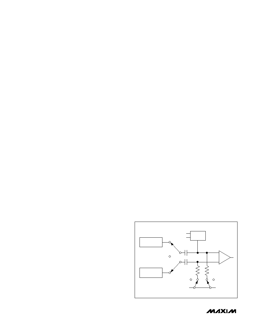
+
-
HOLD
CIN+
REF
GND
DAC
CIN-
VDD/2
COMPARATOR
AIN0–AIN15
GND
HOLD
Figure 3. Equivalent Input Circuit
相关PDF资料 |
PDF描述 |
|---|---|
| MAX11645EUA+T | IC ADC 12BIT I2C/SRL 1CH 8UMAX |
| MAX11647EUA+T | IC ADC 10BIT I2C 94.4KSPS 8UMAX |
| MAX1166BEUP+ | IC ADC 16BIT 165KSPS 20-TSSOP |
| MAX1168BCEG+ | IC ADC 16BIT 200KSPS 24-QSOP |
| MAX1183ECM+TD | IC ADC 10BIT 40MSPS DL 48-TQFP |
相关代理商/技术参数 |
参数描述 |
|---|---|
| MAX11644 | 制造商:MAXIM 制造商全称:Maxim Integrated Products 功能描述:2.7V to 3.6V and 4.5V to 5.5V, Low-Power, 1-/2-Channel, 2-Wire Serial, 12-Bit ADCs |
| MAX11644EUA+ | 功能描述:模数转换器 - ADC 12-Bit 2Ch 94.4ksps 5.5V Precision ADC RoHS:否 制造商:Texas Instruments 通道数量:2 结构:Sigma-Delta 转换速率:125 SPs to 8 KSPs 分辨率:24 bit 输入类型:Differential 信噪比:107 dB 接口类型:SPI 工作电源电压:1.7 V to 3.6 V, 2.7 V to 5.25 V 最大工作温度:+ 85 C 安装风格:SMD/SMT 封装 / 箱体:VQFN-32 |
| MAX11644EUA+T | 功能描述:模数转换器 - ADC 12-Bit 2Ch 94.4ksps 5.5V Precision ADC RoHS:否 制造商:Texas Instruments 通道数量:2 结构:Sigma-Delta 转换速率:125 SPs to 8 KSPs 分辨率:24 bit 输入类型:Differential 信噪比:107 dB 接口类型:SPI 工作电源电压:1.7 V to 3.6 V, 2.7 V to 5.25 V 最大工作温度:+ 85 C 安装风格:SMD/SMT 封装 / 箱体:VQFN-32 |
| MAX11645EUA+ | 功能描述:模数转换器 - ADC 12-Bit 2Ch 94.4ksps 3.6V Precision ADC RoHS:否 制造商:Texas Instruments 通道数量:2 结构:Sigma-Delta 转换速率:125 SPs to 8 KSPs 分辨率:24 bit 输入类型:Differential 信噪比:107 dB 接口类型:SPI 工作电源电压:1.7 V to 3.6 V, 2.7 V to 5.25 V 最大工作温度:+ 85 C 安装风格:SMD/SMT 封装 / 箱体:VQFN-32 |
| MAX11645EUA+T | 功能描述:模数转换器 - ADC 12-Bit 2Ch 94.4ksps 3.6V Precision ADC RoHS:否 制造商:Texas Instruments 通道数量:2 结构:Sigma-Delta 转换速率:125 SPs to 8 KSPs 分辨率:24 bit 输入类型:Differential 信噪比:107 dB 接口类型:SPI 工作电源电压:1.7 V to 3.6 V, 2.7 V to 5.25 V 最大工作温度:+ 85 C 安装风格:SMD/SMT 封装 / 箱体:VQFN-32 |
发布紧急采购,3分钟左右您将得到回复。